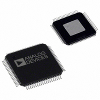
AD9852ASVZ Analog Devices Inc, AD9852ASVZ Datasheet - Page 38

AD9852ASVZ
Manufacturer Part Number
AD9852ASVZ
Description
IC DDS SYNTHESIZER CMOS 80-TQFP
Manufacturer
Analog Devices Inc
Datasheet
1.AD9852ASTZ.pdf
(52 pages)
Specifications of AD9852ASVZ
Resolution (bits)
12 b
Master Fclk
300MHz
Tuning Word Width (bits)
48 b
Voltage - Supply
3.14 V ~ 3.47 V
Operating Temperature
-40°C ~ 85°C
Mounting Type
Surface Mount
Package / Case
80-TQFP Exposed Pad, 80-eTQFP, 80-HTQFP, 80-VQFP
Transmitting Current
815mA
Rf Ic Case Style
TQFP
No. Of Pins
80
Supply Voltage Range
3.135V To 3.465V
Operating Temperature Range
-40°C To +85°C
Msl
MSL 3 - 168 Hours
Frequency Max
300MHz
Lead Free Status / RoHS Status
Lead free / RoHS Compliant
For Use With
AD9852/PCBZ - BOARD EVAL FOR AD9852
Lead Free Status / Rohs Status
Compliant
Available stocks
Company
Part Number
Manufacturer
Quantity
Price
Company:
Part Number:
AD9852ASVZ
Manufacturer:
ADI
Quantity:
263
Company:
Part Number:
AD9852ASVZ
Manufacturer:
Analog Devices Inc
Quantity:
10 000
Part Number:
AD9852ASVZ
Manufacturer:
ADI/亚德诺
Quantity:
20 000
AD9852
POWER DISSIPATION AND THERMAL CONSIDERATIONS
The AD9852 is a multifunctional, high speed device that targets
a wide variety of synthesizer and agile clock applications. The
numerous innovative features contained in the device each
consume incremental power. If enabled in combination, the safe
thermal operating conditions of the device may be exceeded.
Careful analysis and consideration of power dissipation and
thermal management is a critical element in the successful
application of the AD9852 device.
The AD9852 device is specified to operate within the industrial
temperature range of –40°C to +85°C. This specification is con-
ditional, however, such that the absolute maximum junction
temperature of 150°C is not exceeded. At high operating tem-
peratures, extreme care must be taken when operating the device
to avoid exceeding the junction temperature and potentially
damaging the device.
Many variables contribute to the operating junction temperature
within the device, including
•
•
•
•
•
The combination of these variables determines the junction
temperature within the AD9852 device for a given set of
operating conditions.
The AD9852 device is available in two package styles: a
thermally enhanced surface-mount package with an exposed
heat sink and a standard (nonthermally enhanced) surface-
mount package. The thermal impedance of these packages is
16°C/W and 38°C/W, respectively, measured under still air
conditions.
THERMAL IMPEDANCE
The thermal impedance of a package can be thought of as a
thermal resistor that exists between the semiconductor surface
and the ambient air. The thermal impedance is determined by
the package material and the physical dimensions of the package.
The dissipation of the heat from the package is directly depen-
dent on the ambient air conditions and the physical connection
made between the IC package and the PCB.
Adequate dissipation of power from the AD9852 relies on all
power and ground pins of the device being soldered directly to a
copper plane on a PCB. In addition, the thermally enhanced
package of the AD9852ASVZ has an exposed paddle on the
bottom that must be soldered to a large copper plane, which,
for convenience, can be the ground plane. Sockets for either
package style of the AD9852 device are not recommended.
Package style
Selected mode of operation
Internal system clock speed
Supply voltage
Ambient temperature
Rev. E | Page 38 of 52
JUNCTION TEMPERATURE CONSIDERATIONS
The power dissipation (P
application is determined by many operating conditions. Some
of the conditions have a direct relationship with P
supply voltage and clock speed, but others are less deterministic.
The total power dissipation within the device and its effect on
the junction temperature must be considered when using the
device. The junction temperature of the device is given by
The maximum ambient temperature combined with the
maximum junction temperature establish the following power
consumption limits for each package: 4.06 W for ASVZ models
and 1.71 W for ASTZ models.
Supply Voltage
Because P
and junction temperature. Users should design for 3.3 V nominally;
however, the device is guaranteed to meet specifications over the
full temperature range and over the supply voltage range of
3.135 V to 3.465 V.
Clock Speed
Clock speed directly and linearly influences the total power
dissipation of the device and therefore the junction temperature.
As a rule, the user should select the lowest internal clock speed
possible to support a given application to minimize power
dissipation. Typically, the usable frequency output bandwidth
from a DDS is limited to 40% of the clock rate to ensure that the
requirements on the output low-pass filter are reasonable. For a
typical DDS application, the system clock frequency should be
2.5 times the highest desired output frequency.
Mode of Operation
The selected mode of operation for the AD9852 significantly
influences the total power consumption. The AD9852 offers
many features and modes, each of which imposes an additional
power requirement. The available features make the AD9852
suitable for a variety of applications, but the device is designed
to operate with only a few features enabled in a given application.
Enabling multiple features at high clock speeds may result in
exceeding the maximum junction temperature of the die and
therefore severely limit the long-term reliability of the device.
Figure 59 and Figure 60 show the power requirements associated
with each feature of the AD9852. These charts should be used
as a guide when determining how to optimize the AD9852 for
reliable operation in a specific application.
Figure 59 shows the supply current consumed by the AD9852
over a range of frequencies for two possible configurations. All
circuits enabled means that the output scaling multipliers, the
Junction Temperature = (Thermal Impedance ×
Power Consumption) + Ambient Temperature
DISS
= V × I, the supply voltage affects power dissipation
DISS
) of the AD9852 device in a given
DISS
, such as


