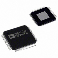
AD9852ASVZ Analog Devices Inc, AD9852ASVZ Datasheet - Page 40

AD9852ASVZ
Manufacturer Part Number
AD9852ASVZ
Description
IC DDS SYNTHESIZER CMOS 80-TQFP
Manufacturer
Analog Devices Inc
Datasheet
1.AD9852ASTZ.pdf
(52 pages)
Specifications of AD9852ASVZ
Resolution (bits)
12 b
Master Fclk
300MHz
Tuning Word Width (bits)
48 b
Voltage - Supply
3.14 V ~ 3.47 V
Operating Temperature
-40°C ~ 85°C
Mounting Type
Surface Mount
Package / Case
80-TQFP Exposed Pad, 80-eTQFP, 80-HTQFP, 80-VQFP
Transmitting Current
815mA
Rf Ic Case Style
TQFP
No. Of Pins
80
Supply Voltage Range
3.135V To 3.465V
Operating Temperature Range
-40°C To +85°C
Msl
MSL 3 - 168 Hours
Frequency Max
300MHz
Lead Free Status / RoHS Status
Lead free / RoHS Compliant
For Use With
AD9852/PCBZ - BOARD EVAL FOR AD9852
Lead Free Status / Rohs Status
Compliant
Available stocks
Company
Part Number
Manufacturer
Quantity
Price
Company:
Part Number:
AD9852ASVZ
Manufacturer:
ADI
Quantity:
263
Company:
Part Number:
AD9852ASVZ
Manufacturer:
Analog Devices Inc
Quantity:
10 000
Part Number:
AD9852ASVZ
Manufacturer:
ADI/亚德诺
Quantity:
20 000
AD9852
EVALUATION OF OPERATING CONDITIONS
The first step in applying the AD9852 is to select the internal
clock frequency. Clock frequency selections greater than 200 MHz
require use of the thermally enhanced package (AD9852ASVZ);
clock frequency selections equal to or less than 200 MHz may
allow use of the standard (nonthermally enhanced) plastic
surface-mount package, but more information is needed to
make this determination.
The second step is to determine the maximum required
operating temperature for the AD9852 in a given application.
Subtract this value from 150°C, which is the maximum junction
temperature allowed for the AD9852. For the extended indust-
rial temperature range, the maximum operating temperature is
85°C, which results in a difference of 65°C. This is the maxi-
mum temperature gradient the device can experience due to
power dissipation.
The third step is to divide this maximum temperature gradient
by the thermal impedance to determine the maximum power
dissipation allowed for the application. For this example, 65°C
divided by the thermal impedance of the package yields a total
Rev. E | Page 40 of 52
power dissipation limit of 4.1 W and 1.7 W for the thermally and
nonthermally enhanced packages, respectively. Therefore, for a
3.3 V nominal power supply voltage, the current consumed by the
device under full operating conditions must not exceed 515 mA
for the standard plastic package or 1242 mA for the thermally
enhanced package. The total set of enabled functions and
operating conditions for a given application must support these
current consumption limits.
Figure 59 and Figure 60 can be used to determine the suitability
of a given AD9852 application in terms of the power dissipation
requirements. These graphs assume that the AD9852 device is
soldered to a multilayer PCB according to the recommended best
manufacturing practices and procedures for a given package type.
This ensures that the specified thermal impedance specifications
are achieved.
THERMALLY ENHANCED PACKAGE
MOUNTING GUIDELINES
Refer to the
devices with an exposed paddle.
AN-772 Application Note
for details on mounting


