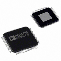
AD9852ASVZ Analog Devices Inc, AD9852ASVZ Datasheet - Page 41

AD9852ASVZ
Manufacturer Part Number
AD9852ASVZ
Description
IC DDS SYNTHESIZER CMOS 80-TQFP
Manufacturer
Analog Devices Inc
Datasheet
1.AD9852ASTZ.pdf
(52 pages)
Specifications of AD9852ASVZ
Resolution (bits)
12 b
Master Fclk
300MHz
Tuning Word Width (bits)
48 b
Voltage - Supply
3.14 V ~ 3.47 V
Operating Temperature
-40°C ~ 85°C
Mounting Type
Surface Mount
Package / Case
80-TQFP Exposed Pad, 80-eTQFP, 80-HTQFP, 80-VQFP
Transmitting Current
815mA
Rf Ic Case Style
TQFP
No. Of Pins
80
Supply Voltage Range
3.135V To 3.465V
Operating Temperature Range
-40°C To +85°C
Msl
MSL 3 - 168 Hours
Frequency Max
300MHz
Lead Free Status / RoHS Status
Lead free / RoHS Compliant
For Use With
AD9852/PCBZ - BOARD EVAL FOR AD9852
Lead Free Status / Rohs Status
Compliant
Available stocks
Company
Part Number
Manufacturer
Quantity
Price
Company:
Part Number:
AD9852ASVZ
Manufacturer:
ADI
Quantity:
263
Company:
Part Number:
AD9852ASVZ
Manufacturer:
Analog Devices Inc
Quantity:
10 000
Part Number:
AD9852ASVZ
Manufacturer:
ADI/亚德诺
Quantity:
20 000
EVALUATION BOARD
An evaluation board is available that supports the AD9852 DDS
device. This evaluation board consists of a PCB, software, and
documentation to facilitate bench analysis of the performance of
the AD9852 device. It is recommended that users of the AD9852
familiarize themselves with the operation and performance
capabilities of the device by using the evaluation board. The
evaluation board should also be used as a PCB reference design
to ensure optimum dynamic performance from the device.
EVALUATION BOARD INSTRUCTIONS
The AD9852/AD9854 Rev. E evaluation board includes either
an AD9852ASVZ or AD9854ASVZ IC.
The ASVZ package permits 300 MHz operation by virtue of its
thermally enhanced design. This package has a bottom-side
heat slug that must be soldered to the ground plane of the
PCB directly beneath the IC. In this manner, the evaluation
board PCB ground plane layer extracts heat from the AD9852
or
or less, the ASTZ package can be used without a heat slug in
customer installations over the full temperature range.
Evaluation boards for both the AD9852 and
identical except for the installed IC.
To assist in proper placement of the pin header shorting
jumpers, the instructions refer to direction (left, right, top,
bottom) as well as header pins to be shorted. Pin 1 for each
3-pin header is marked on the PCB corresponding with the
schematic diagram. When following these instructions, position
the PCB so that the PCB text can be read from left to right. The
board is shipped with the pin headers configuring the board as
follows:
•
•
•
•
•
AD9854
REFCLK for the AD9852 or
differential. The differential clock signals are provided by
the MC100LVEL16D differential receiver.
Input clock for the MC100LVEL16D is single ended via
J25. This signal may be 3.3 V CMOS or a 2 V p-p sine wave
capable of driving 50 Ω (R13).
Both DAC outputs from the AD9852 or
routed through the two 120 MHz elliptical LP filters, and
their outputs are connected to J7 (Q, or control DAC) and
J6 (I , or cosine DAC).
The board is set up for software control via the printer port
connector.
The output currents of the DAC are configured for 10 mA.
IC package. If device operation is limited to 200 MHz
AD9854
is configured as
AD9854
AD9854
are
are
Rev. E | Page 41 of 52
GENERAL OPERATING INSTRUCTIONS
Load the CD software onto the PC’s hard disk. Connect a
printer cable from the PC to the AD9852 evaluation board
printer port connector labeled J11. The current software
(Version 1.72) supports Windows® 95 or better operating
systems.
Hardware Preparation
Using the schematic in conjunction with these instructions
helps acquaint the user with the electrical functioning of the
evaluation board.
Attach power wires to the connector labeled TB1 using the
screw-down terminals. This is a plastic connector that press-fits
over a 4-pin header soldered to the board. Table 14 lists the
connections to each pin.
Table 14. Power Requirements for DUT Pins
AVDD 3.3 V
All DUT
analog pins
1
Clock Input, J25
Attach REFCLK to the clock input, J25. This is a single-ended
input that is routed to the MC100LVEL16D for conversion to
differential PECL output. This is accomplished by attaching a 2
V p-p clock or sine wave source to J25. This is a 50 Ω impedance
point set by R13. The input signal is ac-coupled and then biased
to the center-switching threshold of the MC100LVEL16D. To
engage the differential clocking mode of the AD9852, Pin 2 and
Pin 3 (the bottom two pins) of W3 must be connected with a
shorting jumper.
The signal arriving at the AD9852 is called the reference clock.
If the user chooses to engage the on-chip PLL clock multiplier,
this signal is the reference clock for the PLL and the multiplied
PLL output becomes the system clock. If the user chooses to bypass
the PLL clock multiplier, the reference clock that has been supplied
is directly operating the AD9852 and is therefore the system clock.
Three-State Control
Three of the following control or switch headers must be
shorted to allow the provided software to control the evaluation
board via Printer Port Connector J11: W9, W11, W12, W13,
W14, and W15.
DUT = device under test.
DVDD 3.3 V
All DUT
digital pins
VCC 3.3 V
All other
devices
1
AD9852
Ground
All devices


