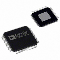
AD9852ASVZ Analog Devices Inc, AD9852ASVZ Datasheet - Page 43

AD9852ASVZ
Manufacturer Part Number
AD9852ASVZ
Description
IC DDS SYNTHESIZER CMOS 80-TQFP
Manufacturer
Analog Devices Inc
Datasheet
1.AD9852ASTZ.pdf
(52 pages)
Specifications of AD9852ASVZ
Resolution (bits)
12 b
Master Fclk
300MHz
Tuning Word Width (bits)
48 b
Voltage - Supply
3.14 V ~ 3.47 V
Operating Temperature
-40°C ~ 85°C
Mounting Type
Surface Mount
Package / Case
80-TQFP Exposed Pad, 80-eTQFP, 80-HTQFP, 80-VQFP
Transmitting Current
815mA
Rf Ic Case Style
TQFP
No. Of Pins
80
Supply Voltage Range
3.135V To 3.465V
Operating Temperature Range
-40°C To +85°C
Msl
MSL 3 - 168 Hours
Frequency Max
300MHz
Lead Free Status / RoHS Status
Lead free / RoHS Compliant
For Use With
AD9852/PCBZ - BOARD EVAL FOR AD9852
Lead Free Status / Rohs Status
Compliant
Available stocks
Company
Part Number
Manufacturer
Quantity
Price
Company:
Part Number:
AD9852ASVZ
Manufacturer:
ADI
Quantity:
263
Company:
Part Number:
AD9852ASVZ
Manufacturer:
Analog Devices Inc
Quantity:
10 000
Part Number:
AD9852ASVZ
Manufacturer:
ADI/亚德诺
Quantity:
20 000
This step reroutes the filtered signals from the output connectors
(J6 and J7) to the 100 Ω configured comparator inputs. This sets
up the comparator for differential input without affecting the
comparator output duty cycle, which should be approximately
50% for the complementary filtered output configuration.
The user can change the value of R
to 1.95 kΩ to receive more robust signals at the comparator
inputs. This decreases jitter and extends the operating range of
the comparator. To implement this change install a shorting
jumper at W6, which provides a second 3.9 kΩ chip resistor
(R20) in parallel with that provided by R2. This boosts the DAC
output current from 10 mA to 20 mA and doubles the peak-to-
peak output voltage developed across the loads, thus resulting
in more robust signals at the comparator inputs.
Single-Ended Configuration
To connect the high speed comparator in a single-ended
configuration so that the duty cycle or pulse width can be
controlled, a dc threshold voltage must be present at one of the
comparator inputs. This voltage can be supplied using the
control DAC. A 12-bit, twos complement value is written to the
control DAC register that sets the IOUT2 output to a static dc
level. Allowable hexadecimal values are 7FF (maximum) to 800
(minimum), with all 0s being midscale. The IOUT1 channel
continues to output a user-programmable, filtered sine wave.
These two signals are routed to the comparator by using the
3-pin W2 and W8 header switches. Use of the configuration
described in the Observing the Filtered IOUT1 and the Filtered
IOUT2 section is required. Follow Step 1 through Step 4 in this
section, and then install a shorting jumper on Pin 1 and Pin 2
(top two pins) of the 3-pin W2 and W8 header switches.
The user can change the value of R
to 1.95 kΩ to receive more robust signals at the comparator
inputs. This decreases jitter and extends the operating range of the
comparator. To implement this change install a shorting jumper
at W6, which provides a second 3.9 kΩ chip resistor (R20) in
parallel with that provided by R2.
USING THE PROVIDED SOFTWARE
The evaluation software is provided on a CD, along with a brief
set of instructions. Use the instructions in conjunction with the
AD9852 or
evaluation board schematic.
The CD-ROM contains the following:
•
•
•
•
•
The AD9852/AD9854 evaluation software
AD9852 evaluation board instructions
AD9852 data sheet
AD9852 evaluation board schematics
AD9852 PCB layout
AD9854
data sheet and the AD9852 or
SET
SET
Resistor R2 from 3.9 kΩ
Resistor R2 from 3.9 kΩ
AD9854
Rev. E | Page 43 of 52
Several numerical entries, such as frequency and phase infor-
mation, require pressing ENTER to register this information.
For example, if a new frequency is input but does not take effect
when Load is clicked, the user probably neglected to press
ENTER after inputting the new frequency information.
Typical operation of the AD9852/AD9854 evaluation board
begins with a master reset. After this reset, many of the default
register values are depicted in the software control panel. The
reset command sets the DDS output amplitude to minimum
and 0 Hz, zero phase offset, as well as other states that are listed
in the Register Layout table (Table 9).
The next programming block should be the reference clock and
multiplier because this information is used to determine the
proper 48-bit frequency tuning words that are entered and later
calculated.
The output amplitude defaults to the 12-bit, straight binary
multiplier values of the I (cosine DAC) multiplier register of
000 hex; no output (dc) should be seen from the DAC. Set the
multiplier amplitude in the Output Amplitude dialog box to a
substantial value, such as FFF hex. The digital multiplier can be
bypassed by selecting the Output Amplitude is always Full Scale
box, but this usually does not result in the best spurious-free
dynamic range (SFDR). The best SFDR, achieving improvements
of up to 11 dB, is obtained by routing the signal through the digital
multiplier and reducing the multiplier amplitude. For instance,
FC0 hex produces less spurious signal amplitude than FFF hex.
If SFDR must be maximized, this exploitable and repeatable
phenomenon should be investigated in the given application.
This phenomenon is more readily observed at higher output
frequencies, where good SFDR becomes more difficult to achieve.
Refer to this data sheet and the evaluation board schematic
(Figure 61 and Figure 62) for information about the available
functions of the AD9852 and how the software responds to
programming commands.
SUPPORT
Applications assistance is available for the AD9852, the AD9852
evaluation board, and all other products of Analog Devices. Call
1-800-ANALOGD or visit www.analog.com/dds.
AD9852


