DS3695AMX/NOPB National Semiconductor, DS3695AMX/NOPB Datasheet
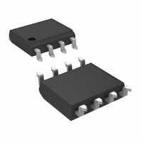
IC TXRX MULT PT RS485/422 8SOIC

DS3695AMX/NOPB

Manufacturer Part Number
DS3695AMX/NOPB
Description
IC TXRX MULT PT RS485/422 8SOIC
Manufacturer
National Semiconductor
Type
Transceiverr
Datasheet

Specifications of DS3695AMX/NOPB

Package / Case
8-SOIC (3.9mm Width)
Mounting Type
Surface Mount
Voltage - Supply
4.75 V ~ 5.25 V
Number Of Drivers/receivers
1/1
Protocol
RS422, RS485
Leaded Process Compatible
Yes
Rohs Compliant
Yes
Peak Reflow Compatible (260 C)
Yes
Data Rate
10Mbps
Number Of Receivers
1
Number Of Transmitters
1
Number Of Transceivers
1
Data Transmission Topology
Multidrop/Multipoint
Receiver Signal Type
Differential
Transmitter Signal Type
Differential
Single Supply Voltage (typ)
5V
Single Supply Voltage (min)
4.75V
Single Supply Voltage (max)
5.25V
Dual Supply Voltage (typ)
Not RequiredV
Dual Supply Voltage (min)
Not RequiredV
Dual Supply Voltage (max)
Not RequiredV
Supply Current
60mA
Power Supply Requirement
Single
Operating Temp Range
0C to 70C
Operating Temperature Classification
Commercial
Mounting
Surface Mount
Pin Count
8
Package Type
SOIC N
Lead Free Status / RoHS Status
Lead free / RoHS Compliant
Other names
DS3695AMXTR
© 2004 National Semiconductor Corporation
DS3695A/DS3695AT/DS3696A
Multipoint RS485/RS422 Transceivers
General Description
The DS3695A and DS3696A are high speed differential
TRI-STATE
quirements of EIA standard RS485 with extended common
mode range (+12V to −7V), for multipoint data transmission.
In addition they are compatible with requirements of RS-422.
The driver and receiver outputs feature TRI-STATE capabil-
ity. The driver outputs remain in TRI-STATE over the entire
common mode range of +12V to −7V. Bus faults that cause
excessive power dissipation within the device trigger a ther-
mal shutdown circuit, which forces the driver outputs into the
high impedance state. The DS3696A provides an output pin
(TS) which reports the thermal shutdown of the device. TS is
an “open collector” pin with an internal 10 kΩ pull-up resistor.
This allows the TS outputs of several devices to be wire
OR-ed.
Both AC and DC specifications are guaranteed over the 0˚C
to 70˚C temperature and 4.75V to 5.25V supply voltage
range.
Connection and Logic Diagram
TS was LF (Line Fault) on previous datasheets, TS goes low upon thermal shutdown.
TRI-STATE
®
is a registered trademark of National Semiconductor Corporation.
®
bus/line transceivers designed to meet the re-
Order Number DS3695AM, DS3695ATM or DS3696AM
DS005272
Molded Package, Small Outline (M)
See NS Package Number M08A
Top View
Top View
Features
n Meets EIA standard RS485 for multipoint bus
n 10 ns driver propagation delays (typical)
n Single +5V supply
n −7V to +12V bus common mode range permits
n Thermal shutdown protection
n High impedance to bus with driver in TRI-STATE or with
n Combined impedance of a driver output and receiver
n 70 mV typical receiver hysteresis
n Available in SOIC packaging
transmission and is compatible with RS-422
ground difference between devices on the bus
power off, over the entire common mode range allows
the unused devices on the bus to be powered down
input is less than one RS485 unit load, allowing up to 32
transceivers on the bus
00527201
00527202
February 1996
www.national.com
±
7V

Related parts for DS3695AMX/NOPB

DS3695AMX/NOPB Summary of contents

Page 1

... Connection and Logic Diagram TS was LF (Line Fault) on previous datasheets, TS goes low upon thermal shutdown. Order Number DS3695AM, DS3695ATM or DS3696AM TRI-STATE ® registered trademark of National Semiconductor Corporation. © 2004 National Semiconductor Corporation Features n Meets EIA standard RS485 for multipoint bus transmission and is compatible with RS-422 ...

Page 2

... Absolute Maximum Ratings If Military/Aerospace specified devices are required, please contact the National Semiconductor Sales Office/ Distributors for availability and specifications. Supply Voltage Control Input Voltages Driver Input Voltage Driver Output Voltages Receiver Input Voltages Receiver Output Voltage @ Continuous Power Dissipation 25˚C ...

Page 3

Note 2: All currents into device pins are positive; all currents out of device pins are negative. All voltages are referenced to device ground unless otherwise specified. Note 3: All typicals are given for and T CC ...

Page 4

AC Test Circuits and Switching Waveforms Differential input voltage may be realized by grounding RI and pulsing RI between +2.5V and −2.5V FIGURE 2. Receiver Input-to-Output Propagation Delay Timing FIGURE 3. Receiver Enable/Disable Propagation Delay Timing Unless otherwise specified the ...

Page 5

AC Test Circuits and Switching Waveforms t and t are measured to the respective 50% points. t PLH PHL FIGURE 5. Driver Input-to-Output Propagation Delay Timing (Single-Ended) FIGURE 6. Driver Enable/Disable Propagation Delay Timing FIGURE 7. Driver Differential Transition Timing ...

Page 6

Function Tables DS3695A/DS3696A Transmitting Inputs DS3695A/DS3696A Receiving — Don’t care condition Z — High impedance state Fault — Improper ...

Page 7

... BANNED SUBSTANCE COMPLIANCE National Semiconductor certifies that the products and packing materials meet the provisions of the Customer Products Stewardship Specification (CSP-9-111C2) and the Banned Substances and Materials of Interest Specification (CSP-9-111S2) and contain no ‘‘Banned Substances’’ as defined in CSP-9-111S2. ...

Related keywords