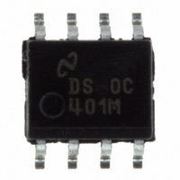
DS90C401M/NOPB National Semiconductor, DS90C401M/NOPB Datasheet

DS90C401M/NOPB
Specifications of DS90C401M/NOPB
*DS90C401M/NOPB
DS90C401M
Available stocks
Related parts for DS90C401M/NOPB
DS90C401M/NOPB Summary of contents
Page 1
... The device lead small outline package. The differential driver outputs provides low EMI with its low output swings typically 340 mV. Connection Diagram Functional Diagram © 2005 National Semiconductor Corporation Features n Ultra low power dissipation n Operates above 155.5 Mbps n Standard TIA/EIA-644 ...
Page 2
... Absolute Maximum Ratings If Military/Aerospace specified devices are required, please contact the National Semiconductor Sales Office/ Distributors for availability and specifications. Supply Voltage ( Input Voltage ( Output Voltage ( OUT+ OUT− Short Circuit Duration ( OUT+ OUT− Maximum Package Power Dissipation M Package Derate M Package 8.5 mW/˚ ...
Page 3
Parameter Measurement Information FIGURE 2. Driver Propagation Delay and Transition Time Test Circuit FIGURE 3. Driver Propagation Delay and Transition Time Waveforms Typical Application FIGURE 1. Driver V and V Test Circuit OD OS FIGURE 4. Point-to-Point Application 3 10001304 ...
Page 4
Applications Information LVDS drivers and receivers are intended to be primarily used in an uncomplicated point-to-point configuration as is shown in Figure 4. This configuration provides a clean signaling environment for the quick edge rates of the drivers. The receiver ...
Page 5
Pin Descriptions TABLE 1. Device Pin Descriptions Pin No. Name Description TTL/CMOS driver input pins Non-inverting driver output pin OUT Inverting driver output pin OUT− 5 GND Ground pin 1 ...
Page 6
Typical Performance Characteristics Power Supply Current vs Power Supply Voltage Output Short Circuit Current vs Power Supply Voltage www.national.com (Continued) Power Supply Current vs Temperature 10001313 Differential Output Voltage vs Power Supply Voltage 10001316 6 10001314 10001317 ...
Page 7
Typical Performance Characteristics Differential Output Voltage vs Ambient Temperature Output Voltage High vs Ambient Temperature (Continued) Output Voltage High vs Power Supply Voltage 10001318 Output Voltage Low vs Power Supply Voltage 10001320 7 10001319 10001321 www.national.com ...
Page 8
Typical Performance Characteristics Output Voltage Low vs Ambient Temperature Offset Voltage vs Ambient Temperature www.national.com (Continued) Offset Voltage vs Power Supply Voltage 10001322 Power Supply Current vs Frequency 10001324 8 10001323 10001325 ...
Page 9
Typical Performance Characteristics Differential Output Voltage vs Load Resistor Differential Propagation Delay vs Ambient Temperature (Continued) Differential Propagation Delay vs Power Supply Voltage 10001327 Differential Skew vs Power Supply Voltage 10001329 9 10001328 10001330 www.national.com ...
Page 10
Typical Performance Characteristics Differential Skew vs Ambient Temperature Differential Transition Time vs Ambient Temperature www.national.com (Continued) Differential Transition Time vs Power Supply Voltage 10001331 10001333 10 10001332 ...
Page 11
... BANNED SUBSTANCE COMPLIANCE National Semiconductor manufactures products and uses packing materials that meet the provisions of the Customer Products Stewardship Specification (CSP-9-111C2) and the Banned Substances and Materials of Interest Specification (CSP-9-111S2) and contain no ‘‘Banned Substances’’ as defined in CSP-9-111S2. ...


