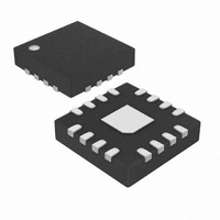
MAX3804ETE#G16 Maxim Integrated Products, MAX3804ETE#G16 Datasheet - Page 2

MAX3804ETE#G16
Manufacturer Part Number
MAX3804ETE#G16
Description
IC EQUALIZER REC 12.5GBPS 16TQFN
Manufacturer
Maxim Integrated Products
Type
Transmitterr
Datasheet
1.MAX3804ETEG16.pdf
(9 pages)
Specifications of MAX3804ETE#G16
Protocol
Ethernet
Voltage - Supply
3 V ~ 3.6 V
Mounting Type
Surface Mount
Package / Case
16-TQFN Exposed Pad
Lead Free Status / RoHS Status
Lead free / RoHS Compliant
Number Of Drivers/receivers
-
Available stocks
Company
Part Number
Manufacturer
Quantity
Price
ABSOLUTE MAXIMUM RATINGS
Supply Voltage (V
CML Supply Voltage (V
Current at Serial Output (SDO+, SDO-) ............................±25mA
Input Voltage (SDI+, SDI-, EQ1,
12.5Gbps Settable Receive Equalizer
Stresses beyond those listed under “Absolute Maximum Ratings” may cause permanent damage to the device. These are stress ratings only, and functional
operation of the device at these or any other conditions beyond those indicated in the operational sections of the specifications is not implied. Exposure to
absolute maximum rating conditions for extended periods may affect device reliability.
ELECTRICAL CHARACTERISTICS
(V
and T
Note 1: Differential Input Sensitivity is defined at the input to a transmission line. The transmission line is differential Z
Note 2: Measured with 0000011111 pattern at 12.5Gbps.
Note 3: Residual jitter is the difference in total jitter (RJ, PWD, and PDJ) between the transmitted signal (at the input to the transmis-
Note 4: Measured at 10.7Gbps using a pattern of 100 ones, 2
Note 5: V
Note 6: Guaranteed by design and characterization.
2
Supply Current
CML Input Differential
CML Input Common Mode
CML Input Termination
CML Input Return Loss
CML Output Differential
CML Output Impedance
CML Output Transition Time
Residual Jitter Output
(Total RJ, PWD, and PDJ)
LVTTL Input Current
LVTTL Input Low
LVTTL Input High
CC
EQ2, EQ3) ..............................................-0.5V to (V
_______________________________________________________________________________________
= +3.0V to +3.6V, V
A
= +25°C, unless otherwise noted.)
microstrip in FR-4, ε
sion line) and equalizer output. Total residual jitter is DJ
Deterministic jitter at the input is from frequency-dependent, media-induced loss only.
IN
PARAMETER
= 400mV
CC
) ............................................-0.5V to +4.0V
P-P
CC1
to 1200mV
CC1
, V
r
CC2
= 4.5, and tan δ = 0.02, V
= V
) ............-0.5V to (V
CC2
P-P
SYMBOL
, input path is 0 to 30in, 6-mil microstrip in FR-4, ε
= +1.65V to +3.6V, T
I
V
t
IH
I
R
V
V
V
OUT
CC
, t
, I
IN
IH
IL
F
IL
AC-coupled or DC-coupled (Note 1)
DC-coupled
Single ended
Up to 5GHz
Single ended
20% to 80% (Notes 2, 6)
At 10.7Gbps (Notes 3, 4, 5, 6)
At 12.5Gbps (Notes 3, 4, 5, 6)
CC
CC
+ 0.5V)
+ 0.5V)
IN
A
= (SDI+ - SDI-).
= -40°C to +85°C. Typical values are at V
7
PRBS, 100 zeros, 2
P-P
CONDITIONS
+ 14.2 x RJ
Continuous Power Dissipation (T
Operating Temperature Range ...........................-40°C to +85°C
Storage Temperature Range .............................-55°C to +150°C
Lead Temperature (soldering, 10s) .................................+300°C
16-Lead Thin QFN-EP (derate 17.5mW/°C
above +85°C) ........................................................1398mW
RMS
7
.
PRBS, and at 12.5Gbps using a K28.5 pattern.
r
= 4.5, and tan δ = 0.02.
V
- 0.4
MIN
42.5
42.5
400
400
-30
2.0
CC1
A
= +85°C)
CC
TYP
500
35
50
10
50
24
17
= V
CC1
MAX
1200
V
+ 0.1
57.5
57.5
= V
+30
600
0.8
0
50
CC1
35
30
30
= 100Ω, 6-mil
CC2
= +3.3V,
UNITS
mV
mV
ps
mA
dB
ps
µA
Ω
Ω
V
V
V
P-P
P-P
P-P


