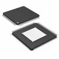
DS26303L-120+ Maxim Integrated Products, DS26303L-120+ Datasheet - Page 15

DS26303L-120+
Manufacturer Part Number
DS26303L-120+
Description
IC LIU E1/T1/J1 3.3V 144-ELQFP
Manufacturer
Maxim Integrated Products
Type
Line Interface Units (LIUs)r
Datasheet
1.DS26303L-120.pdf
(101 pages)
Specifications of DS26303L-120+
Number Of Drivers/receivers
8/8
Protocol
T1/E1/J1
Voltage - Supply
3.135 V ~ 3.465 V
Mounting Type
Surface Mount
Package / Case
144-LQFP Exposed Pad, 144-eLQFP, 144-HLQFP
Maximum Operating Temperature
+ 70 C
Mounting Style
SMD/SMT
Minimum Operating Temperature
0 C
Lead Free Status / RoHS Status
Lead free / RoHS Compliant
SDI/WRB/DSB/TS0
RDB/RWB/TS1
SCLK/ALE/
ASB/TS2
NAME
PIN
86
85
84
TYPE
I
I
I
DS26303: 3.3V, T1/E1/J1, Short-Haul, Octal Line Interface Unit
Serial Clock/Address Latch Enable/Address Strobe
Bar/Template Selection 2
SCLK: In the serial host mode, this pin is the serial clock. Data on
SDI is clocked on the rising edge of SCLK. The data is clocked on
SDO on the rising edge of SCLK if CLKE is high. If CLKE is low
the data on SDO is clocked on the falling edge of SCLK.
ALE: In parallel Intel multiplexed mode, the address lines are
latched on the falling edge of ALE. Tie ALE pin high if using
nonmultiplexed mode.
ASB: In parallel Motorola multiplexed mode, the address is
sampled on the falling edge of ASB. Tie ASB pin high if using
nonmultiplexed mode.
TS2: In hardware mode, this pin signal is one of the template
selection bits. See
Read Bar/Read Write Bar/Template Selection 1
RDB: In Intel host mode, this pin must be low for read operation.
RWB: In Motorola mode, this pin is low for write operation and
high for read operation.
TS1: In hardware mode, this pin signal is one of the template
selection bits. See
Serial Data Input/Write Bar/Data Strobe Bar/Template
Selection 0
SDI: In the serial host mode, this pin is the serial input SDI. It is
sampled on the rising edge of SCLK. Data is input LSB first.
WRB: In Intel host mode, this pin is active low during write
operation. The data is sampled on the rising edge of WRB.
DSB: In the parallel Motorola mode, this pin is active low. During a
write operation the data is sampled on the rising edge of DSB.
During a read operation the data (D[7:0] or AD[7:0]) is driven on
the falling edge of DSB. In the nonmultiplexed Motorola mode, the
address bus (A[5:0]) is latched on the falling edge of DSB.
TS0: In hardware mode, this pin signal is one of the template
select bits. See
15 of 101
Table
Table
Table
5-11.
5-11.
5-11.
FUNCTION


