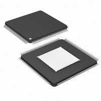
DS26303L-120+ Maxim Integrated Products, DS26303L-120+ Datasheet - Page 76

DS26303L-120+
Manufacturer Part Number
DS26303L-120+
Description
IC LIU E1/T1/J1 3.3V 144-ELQFP
Manufacturer
Maxim Integrated Products
Type
Line Interface Units (LIUs)r
Datasheet
1.DS26303L-120.pdf
(101 pages)
Specifications of DS26303L-120+
Number Of Drivers/receivers
8/8
Protocol
T1/E1/J1
Voltage - Supply
3.135 V ~ 3.465 V
Mounting Type
Surface Mount
Package / Case
144-LQFP Exposed Pad, 144-eLQFP, 144-HLQFP
Maximum Operating Temperature
+ 70 C
Mounting Style
SMD/SMT
Minimum Operating Temperature
0 C
Lead Free Status / RoHS Status
Lead free / RoHS Compliant
7.2 Instruction Register
The instruction register contains a shift register as well as a latched parallel output and is 3 bits in length. When the
TAP controller enters the Shift-IR state, the instruction shift register will be connected between JTDI and JTDO.
While in the Shift-IR state, a rising edge on TCLK with JTMS LOW will shift the data one stage towards the serial
output at JTDO. A rising edge on TCLK in the Exit1-IR state or the Exit2-IR state with JTMS HIGH will move the
controller to the Update-IR state. The falling edge of that same TCLK will latch the data in the instruction shift
register to the instruction parallel output. Instructions supported by the DS26303 and its respective operational
binary codes are shown in
Table 7-1. Instruction Codes for IEEE 1149.1 Architecture
7.2.1 EXTEST
This allows testing of all interconnections to the device. When the EXTEST instruction is latched in the instruction
register, the following actions occur. Once enabled via the Update-IR state, the parallel outputs of all digital output
pins will be driven. The Boundary Scan Register will be connected between JTDI and JTDO. The Capture-DR will
sample all digital inputs into the Boundary Scan Register.
7.2.2 HIGHZ
All digital outputs of the device will be placed in a high-impedance state. The Bypass Register will be connected
between JTDI and JTDO.
7.2.3 CLAMP
All digital outputs of the device will output data from the boundary scan parallel output while connecting the Bypass
Register between JTDI and JTDO. The outputs will not change during the CLAMP instruction.
7.2.4
This is a mandatory instruction for the IEEE 1149.1 specification that supports two functions. The digital I/Os of the
device can be sampled at the Boundary Scan Register without interfering with the normal operation of the device
by using the Capture-DR state. SAMPLE/PRELOAD also allows the device to shift data into the Boundary Scan
Register via JTDI using the Shift-DR state.
7.2.5 IDCODE
When the IDCODE instruction is latched into the parallel instruction register, the identification test register is
selected. The device identification code will be loaded into the identification register on the rising edge of TCLK
following entry into the Capture-DR state. Shift-DR can be used to shift the identification code out serially via
JTDO. During Test-Logic-Reset, the identification code is forced into the instruction register’s parallel output. The
ID code will always have a 1 in the LSB position. The next 11 bits identify the manufacturer’s JEDEC number and
number of continuation bytes followed by 16 bits for the device and 4 bits for the version
the device ID code for the DS26303.
7.2.6 BYPASS
When the BYPASS instruction is latched into the parallel instruction register, JTDI connects to JTDO through the
1-bit bypass test register. This allows data to pass from JTDI to JTDO without affecting the device’s normal
operation.
SAMPLE/PRELOAD
INSTRUCTION
SAMPLE/PRELOAD
BYPASS
EXTEST
IDCODE
CLAMP
HIGHZ
Table
7-1.
SELECTED REGISTER
Device Identification
Boundary Scan
Boundary Scan
Bypass
Bypass
Bypass
DS26303: 3.3V, T1/E1/J1, Short-Haul, Octal Line Interface Unit
76 of 101
INSTRUCTION CODES
000
010
011
100
110
111
Table
7-2.
Table 7-3
lists


