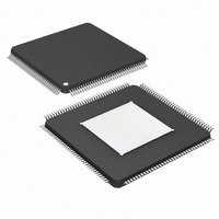
DS26303LN-120+ Maxim Integrated Products, DS26303LN-120+ Datasheet - Page 17

DS26303LN-120+
Manufacturer Part Number
DS26303LN-120+
Description
IC LIU E1/T1/J1 3.3V 144-ELQFP
Manufacturer
Maxim Integrated Products
Type
Line Interface Units (LIUs)r
Datasheet
1.DS26303L-120.pdf
(101 pages)
Specifications of DS26303LN-120+
Number Of Drivers/receivers
8/8
Protocol
T1/E1/J1
Voltage - Supply
3.135 V ~ 3.465 V
Mounting Type
Surface Mount
Package / Case
144-LQFP Exposed Pad, 144-eLQFP, 144-HLQFP
Maximum Operating Temperature
+ 85 C
Mounting Style
SMD/SMT
Minimum Operating Temperature
- 40 C
Lead Free Status / RoHS Status
Lead free / RoHS Compliant
A4/RIMPMSB
A3/GMC3
A2/GMC2
A1/GMC1
A0/GMC0
JTRSTB
JTCLK
NAME
CLKE
JTMS
JTDO
JTDI
OE
PIN
114
115
12
13
14
15
16
95
96
97
98
99
I, pullup
I, pullup
I, pullup
high-Z
TYPE
O,
I
I
I
I
DS26303: 3.3V, T1/E1/J1, Short-Haul, Octal Line Interface Unit
Address Bus 4–0/G.772 Monitoring Control/Rx Impedance
Mode Select
A[4:0]: These five pins are address pins in parallel host mode. In
serial host mode and multiplexed host mode, these pins should be
grounded.
RIMPMSB: In hardware mode when this pin is low, the internal
impedance mode is selected, so all RTIP and RING pins require
no external resistance component. When high, external
impedance mode is selected so all RTIP and RING pins require
external resistance.
GMC[3:0]: In hardware mode, these signal pins are used to select
a transmit line (TTIPn/TRINGn) or receive line (RTIPn/RRINGn)
for nonintrusive monitoring. Receiver 1 is used to monitor
channels 2 to 8 See
Output Enable. If this pin is pulled low, all the transmitter outputs
(TTIPn and TRINGn) are high impedance. Additionally, the user
may use this same pin to turn off all the impedance matching for
the receivers at the same time if register bit GMR.RHPMC is set.
Clock Edge. When CLKE is high, SDO is valid on the falling edge
of SCLK. When CLKE is low SDO is valid on the rising edge of
SCLK. When CLKE is high, the RCLKn for all the channels is
inverted. This aligns RPOSn/RNEGn on the falling edge of RCLKn
and overrides the settings in register RCLKI. When low,
RPOSn/RNEGn is aligned according to the settings in register
RCLKI.
JTAG Test Port Reset. This pin if low resets the JTAG port. If not
used it can be left floating.
JTAG Test Mode Select. This pin is clocked on the rising edge of
JTCLK and is used to control the JTAG selection between scan
and test machine control.
JTAG Test Clock. The data JTDI and JTMS are clocked on rising
edge of JTCLK and JTDO is clocked out on the falling edge of
JTCLK.
JTAG Test Data Out. This is the serial output of the JTAG port.
The data is clocked out on the falling edge of JTCLK.
Test Data Input. This pin input is the serial data of the JTAG test.
The data on JTDI is clocked on the rising edge of JTCLK. This pin
can be left unconnected.
17 of 101
JTAG
Table
5-9.
FUNCTION


