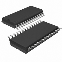
LT1537CSW Linear Technology, LT1537CSW Datasheet - Page 3

LT1537CSW
Manufacturer Part Number
LT1537CSW
Description
IC TXRX 5V RS232 LOW-PWR 28-SOIC
Manufacturer
Linear Technology
Type
Transceiverr
Datasheet
1.LT1537CSW.pdf
(8 pages)
Specifications of LT1537CSW
Number Of Drivers/receivers
3/5
Protocol
RS232
Voltage - Supply
4.5 V ~ 5.5 V
Mounting Type
Surface Mount
Package / Case
28-SOIC (7.5mm Width)
Lead Free Status / RoHS Status
Contains lead / RoHS non-compliant
Available stocks
Company
Part Number
Manufacturer
Quantity
Price
Part Number:
LT1537CSW
Manufacturer:
LINEAR/凌特
Quantity:
20 000
Part Number:
LT1537CSW#PBF
Manufacturer:
LINEAR/凌特
Quantity:
20 000
Part Number:
LT1537CSW#TRPBF
Manufacturer:
LINEAR/凌特
Quantity:
20 000
TYPICAL PERFOR
ELECTRICAL C
PARAMETER
Any Driver
Output Leakage Current
Data Rate
Slew Rate
Propagation Delay
Any Receiver
Input Voltage Thresholds
Hysteresis
Input Resistance
Output Voltage
Output Leakage Current
Output Short-Circuit Current
Propagation Delay
The
range (0 C T
industrial grade).
Note 1: Absolute Maximum Ratings are those values beyond which the life
of the device may be impaired.
Note 2: Testing done at V
C
Note 3: Supply current is measured with driver and receiver outputs
unloaded and the driver inputs tied high.
Note 4: Supply current and leakage current measurements in shutdown
are performed with V
DRIVER DISABLE are performed with V
+
–10
–2
–4
–6
–8
10
= C
8
6
4
2
0
–50
Driver Output Voltage
denotes specifications which apply over the operating temperature
–
= 0.1 F.
V
–25
CC
V
V
CC
CC
= 5.5V
A
= 5V
= 5.5V
0
TEMPERATURE ( C)
70 C for commercial grade and – 40 C T
OUTPUT HIGH
OUTPUT LOW
ON/OFF
25
V
CC
CC
= 5V
V
50
= 5V and V
= 0.1V. Supply current measurements using
CC
V
CC
HARA TERISTICS
= 4.5V
= 4.5V
75
W
R
LT1537 • TPC01
L
100
ON/OFF
= 3k
DRIVER DISABLE
A
C
CONDITIONS
Shutdown V
R
R
R
R
Output Transition t
Output Transition t
Input LOW Threshold (V
Input HIGH Threshold (V
V
Output LOW, I
Output HIGH, I
Shutdown (Note 4) 0 V
Sinking Current, V
Sourcing Current, V
Output Transition t
Output Transition t
U
125
L
L
L
L
IN
= 3V. C1 = C2 = 0.2 F,
= 3k, C
= 3k, C
= 3k, C
= 3k, C
= 10V
CE
L
L
L
L
C
= 3V.
= 2500pF
= 1000pF
= 51pF
= 2500pF
OUT
2.00
0.50
HARA TERISTICS
3.00
2.75
2.50
2.25
1.75
1.50
1.25
1.00
0.75
OUT
OUT
= 15V (Note 4)
–55
Receiver Input Thresholds
OUT
A
= – 1.6mA
HL
LH
HL
LH
= 160 A (V
OUT
HIGH to LOW (Note 5)
LOW to HIGH
HIGH to LOW (Note 6)
LOW to HIGH
–25
85 C for
= V
= 0V
OUT
OUT
OUT
C
CC
(Note 2)
= HIGH)
0
= LOW)
TEMPERATURE ( C)
CC
V
INPUT HIGH
INPUT LOW
CC
= 5V)
25
Note 5: For driver delay measurements, R
points are set between the driver’s input logic threshold and the output
transition to the zero crossing (t
Note 6: For receiver delay measurements, C
between the receiver’s input logic threshold and the output transition to
standard TTL/CMOS logic threshold (t
0.8V).
Note 7: Absolute maximum externally applied voltage. Internal charge
pump may force a larger value on this pin.
50
75
ILT1537 • TPC02
100
125
40
80
70
60
50
30
20
10
0
HL
Supply Current vs Data Rate
0
= 1.4V to 0V and t
MIN
3 DRIVERS ACTIVE
R
C
120
250
0.8
0.1
3.5
L
L
4
3
HL
10
= 2500pF
= 3k
25
= 1.3V to 2.4V and t
L
L
= 3k and C
= 51pF. Trigger points are set
DATA RATE (kBAUD)
50
TYP
– 20
250
350
0.6
0.5
1.3
1.7
0.4
0.2
4.2
10
15
15
5
1
20
75
LH
L
= 51pF. Trigger
= 1.4V to 0V).
MAX
100
– 10
600
600
1.3
1.3
2.4
1.0
0.4
30
10
100
7
LT1537
LH
= 1.7V to
LTX1537 • TPC03
125
UNITS
kBaud
kBaud
3
V/ s
V/ s
150
mA
mA
k
ns
ns
A
V
V
V
V
V
A
s
s


