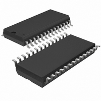
LT1537CSW Linear Technology, LT1537CSW Datasheet - Page 5

LT1537CSW
Manufacturer Part Number
LT1537CSW
Description
IC TXRX 5V RS232 LOW-PWR 28-SOIC
Manufacturer
Linear Technology
Type
Transceiverr
Datasheet
1.LT1537CSW.pdf
(8 pages)
Specifications of LT1537CSW
Number Of Drivers/receivers
3/5
Protocol
RS232
Voltage - Supply
4.5 V ~ 5.5 V
Mounting Type
Surface Mount
Package / Case
28-SOIC (7.5mm Width)
Lead Free Status / RoHS Status
Contains lead / RoHS non-compliant
Available stocks
Company
Part Number
Manufacturer
Quantity
Price
Part Number:
LT1537CSW
Manufacturer:
LINEAR/凌特
Quantity:
20 000
Part Number:
LT1537CSW#PBF
Manufacturer:
LINEAR/凌特
Quantity:
20 000
Part Number:
LT1537CSW#TRPBF
Manufacturer:
LINEAR/凌特
Quantity:
20 000
TYPICAL PERFOR
PI FU CTIO S
V
the shutdown mode. This pin should be decoupled with a
0.1 F ceramic capacitor close to the package pin. Insuffi-
cient supply bypassing can result in low output drive levels
and erratic charge pump operation.
GND: Ground Pin.
ON/OFF: TTL/CMOS Compatible Operating Mode Control.
A logic LOW puts the device in the shutdown mode which
reduces input supply current to zero and places all of the
drivers and receivers in high impedance state. A logic
HIGH fully enables the transceiver.
DRIVER DISABLE: This pin provides an alternate control
for the charge pump and RS232 drivers. A logic HIGH on
this pin shuts down the charge pump and places all drivers
in a high impedance state. Receivers remain active under
these conditions. Floating the driver disable pin or driving
it to a logic LOW level fully enables the transceiver. A logic
LOW on the On/Off pin supersedes the state of the Driver
Disable pin. Supply current drops to 1.5mA when in
DRIVER DISABLE mode.
V
1.5V. This pin requires an external charge storage capaci-
tor C 0.1 F, tied to ground or V
tors may be used to reduce supply ripple. With multiple
transceivers, the V
common capacitors. For large numbers of transceivers,
increasing the size of the shared common storage capaci-
tors is recommended to reduce ripple.
CC
+
: Positive Supply Output (RS232 Drivers). V
U
OUTPUT HIGH
: 5V Input Supply Pin. Supply current drops to zero in
OUTPUT LOW
ON/OFF PIN
DRIVER
DRIVER
R
R
L
L
= 3k
= 3k
U
– 10
– 5
10
5
0
Shutdown to Driver Output
+
U
and V
–
W
pins may be paralleled into
A
CC
U
. Larger value capaci-
CE
C
LT1537 • TPC12
HARA TERISTICS
+
2V
C
CC
–
DRIVER OUTPUT
DRIVER OUTPUT
V
–(2V
storage capacitor C 0.1 F. V
30 seconds.
C1
pins require two external capacitors C 0.2 F: one from
C1
charge pump efficiency, the capacitor’s effective series
resistance should be less than 2 . Low ESR ceramic
capacitors work well in this application.
DRIVER IN: RS232 Driver Input Pins. These inputs are
TTL/CMOS compatible. Inputs should not be allowed to
float. Tie unused inputs to V
DRIVER OUT: Driver Outputs at RS232 Voltage Levels.
Driver output swing meets RS232 levels for loads up to 3k.
Slew rates are controlled for lightly loaded lines. Output
current capability is sufficient for load conditions up to
2500pF. Outputs are in a high impedance state when in
shutdown mode, V
is active. Outputs are fully short-circuit protected from V
+ 25V to V
damage the device if the overdrive is moderately current
limited. Short circuits on one output can load the power
supply generator and may disrupt the signal levels of the
other outputs. The driver outputs are protected against
ESD to 5kV for human body model discharges.
–
C
: Negative Supply Output (RS232 Drivers). V
+
+
L
, C1
= 2500pF
to C1
CC
R
R
L
INPUT
L
= 3k
= 3k
–
– 2.5V). This pin requires an external charge
, C2
–
Driver Output Waveforms
+
and another from C2
+
, C2
– 25V. Applying higher voltages will not
–
: Commutating Capacitor Inputs. These
CC
= 0V or when the driver disable pin
CC
–
.
is short-circuit proof for
+
to C2
LT1537 • TPC13
–
. To maintain
LT1537
–
5
–


