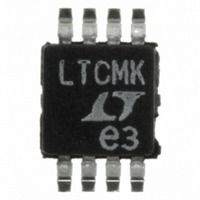
LTC2857CMS8-2#PBF Linear Technology, LTC2857CMS8-2#PBF Datasheet

LTC2857CMS8-2#PBF
Specifications of LTC2857CMS8-2#PBF
Available stocks
Related parts for LTC2857CMS8-2#PBF
LTC2857CMS8-2#PBF Summary of contents
Page 1
... MSOP Packages APPLICATIONS Low Power RS485/RS422 Transceiver ■ Level Translator ■ ■ Backplane Transceiver , LT, LTC and LTM are registered trademarks of Linear Technology Corporation. All other trademarks are the property of their respective owners. TYPICAL APPLICATION LTC2856-1 RO1 V CC1 R ...
Page 2
LTC2857-1/LTC2857-2 LTC2858-1/LTC2858-2 ABSOLUTE MAXIMUM RATINGS (Note 1) Supply Voltage (V ) ................................... –0. Logic Input Voltages (RE, DE, DI) ................ –0. Interface I/O ( ....................(V Receiver Output Voltage (RO) .......–0. ...
Page 3
ORDER INFORMATION LTC2856 #TR PBF Consult LTC Marketing for information on non-standard lead based fi nish parts. For more information on lead free part marking, go to: For more information on tape and reel specifi cations, go ...
Page 4
LTC2857-1/LTC2857-2 LTC2858-1/LTC2858-2 ELECTRICAL CHARACTERISTICS temperature range, otherwise specifi cations are at T SYMBOL PARAMETER Driver |V | Differential Driver Output Voltage OD Δ|V | Change in Magnitude of Driver Differential OD Output Voltage for Complementary Output States V Driver Common ...
Page 5
SWITCHING CHARACTERISTICS temperature range, otherwise specifi cations are at T SYMBOL PARAMETER I Supply Current in Transmit Mode CCT I Supply Current with Both Driver and Receiver CCTR Enabled Driver in LTC2856-1, LTC2857-1, LTC2858-1 f Maximum Data Rate MAX t ...
Page 6
LTC2857-1/LTC2857-2 LTC2858-1/LTC2858-2 ELECTRICAL CHARACTERISTICS Note 1: Stresses beyond those listed under Absolute Maximum Ratings may cause permanent damage to the device. Exposure to any Absolute Maximum Rating condition for extended periods may affect device reliability and lifetime. High temperatures degrade ...
Page 7
TEST CIRCUITS Y DI DRIVER R DIFF Z 285678 F04a DRIVER GND Figure 5. Driver Enable and Disable Timing Measurement Y-Z ...
Page 8
LTC2857-1/LTC2857-2 LTC2858-1/LTC2858-2 TEST CIRCUITS A ± RECEIVER CM B ± RECEIVER 285678 F07a FUNCTION TABLES LTC2856-1, LTC2856-2 ...
Page 9
TYPICAL PERFORMANCE CHARACTERISTICS Receiver Skew vs Temperature 1. 15pF –1 –40 – 100 120 TEMPERATURE (°C) 385678 G01 Driver Output Short-Circuit Current vs Temperature 160 SOURCE ...
Page 10
LTC2857-1/LTC2857-2 LTC2858-1/LTC2858-2 PIN FUNCTIONS PIN NUMBER LTC2856-1 LTC2857-1 PIN NAME LTC2856-2 LTC2857 GND 5/9* 4/ ...
Page 11
BLOCK DIAGRAMS LTC2856-1, LTC2856-2 RO RECEIVER RE SLEEP/SHUTDOWN LOGIC AND DELAY DE DRIVER (15kV) B (15kV) DI 2856 BD LTC2858-1, LTC2858-2 RO RECEIVER RE SLEEP/SHUTDOWN LOGIC AND DELAY DE DI DRIVER 2858 BD LTC2857-1/LTC2857-2 LTC2858-1/LTC2858-2 LTC2857-1, LTC2857-2 ...
Page 12
LTC2857-1/LTC2857-2 LTC2858-1/LTC2858-2 APPLICATIONS INFORMATION Driver The driver provides full RS485 and RS422 compatibility. When enabled high, Y-Z is positive for the full-duplex devices and A-B is positive for the half-duplex device. When the driver is disabled, both ...
Page 13
APPLICATIONS INFORMATION 54Ω DIFF 1000pF DATA RATE (kbps) Figure 8. Supply Current vs Data Rate High Speed Considerations A ground plane layout is ...
Page 14
LTC2857-1/LTC2857-2 LTC2858-1/LTC2858-2 APPLICATIONS INFORMATION Time-Based Traces Y, Z 1V/DIV Y-Z 2V/DIV 2μs/DIV Figure 10. LTC2858-1 Driver Output at 100kHz Into 100Ω Resistor 14 Y-Z 10dB/DIV 285678 F10a Frequency Spectrum 285678 F10b 1.25MHz/DIV 285678fe ...
Page 15
APPLICATIONS INFORMATION Time-Based Traces Y, Z 1V/DIV Y-Z 2V/DIV 2μs/DIV Figure 11. LTC2858-2 Driver Output at 100kHz Into 100Ω Resistor TYPICAL APPLICATIONS Y-Z 10dB/DIV 285678 F11a Failsafe “0” Application (Idle State = Logic “0” 100k ...
Page 16
LTC2857-1/LTC2857-2 LTC2858-1/LTC2858-2 PACKAGE DESCRIPTION 3.5 0.05 1.65 0.05 2.15 0.05 (2 SIDES) 0.25 0.05 RECOMMENDED SOLDER PAD PITCH AND DIMENSIONS PIN 1 TOP MARK (NOTE 6) 0.200 REF 16 DD Package 8-Lead Plastic DFN (3mm × 3mm) (Reference LTC DWG ...
Page 17
PACKAGE DESCRIPTION 3.50 0.05 1.65 0.05 2.15 0.05 (2 SIDES) 0.25 0.05 0.50 BSC 2.38 0.05 (2 SIDES) RECOMMENDED SOLDER PAD PITCH AND DIMENSIONS NOTE: 1. DRAWING TO BE MADE A JEDEC PACKAGE OUTLINE M0-229 VARIATION OF (WEED-2). CHECK THE ...
Page 18
LTC2857-1/LTC2857-2 LTC2858-1/LTC2858-2 PACKAGE DESCRIPTION 5.23 (.206) MIN 0.42 0.038 (.0165 .0015) TYP RECOMMENDED SOLDER PAD LAYOUT 0.254 (.010) GAUGE PLANE 0.18 (.007) NOTE: 1. DIMENSIONS IN MILLIMETER/(INCH) 2. DRAWING NOT TO SCALE 3. DIMENSION DOES NOT INCLUDE MOLD FLASH, PROTRUSIONS ...
Page 19
... LEAD COPLANARITY (BOTTOM OF LEADS AFTER FORMING) SHALL BE 0.102mm (.004") MAX Information furnished by Linear Technology Corporation is believed to be accurate and reliable. However, no responsibility is assumed for its use. Linear Technology Corporation makes no representa- tion that the interconnection of its circuits as described herein will not infringe on existing patent rights. ...
Page 20
... Up to 256 Transceiver on the Bus Channel-to-Channel Skew 400ps (Typ) 2500V Isolation in Surface Mount Package RMS Propagation Delay Skew 500ps (Typ) 60V Tolerant, ±15kV ESD Integrated, Switchable, 120Ω Termination Resistor, ±15kV ESD LT 0308 REV E • PRINTED IN USA © LINEAR TECHNOLOGY CORPORATION 2006 285678fe ...


