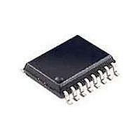
TDA7073ATD NXP Semiconductors, TDA7073ATD Datasheet

TDA7073ATD
Specifications of TDA7073ATD
Related parts for TDA7073ATD
TDA7073ATD Summary of contents
Page 1
DATA SHEET TDA7073A; TDA7073AT Dual BTL power driver Product specification Supersedes data of 1994 July INTEGRATED CIRCUITS 1999 Aug 30 ...
Page 2
... NXP Semiconductors Dual BTL power driver FEATURES • No external components • Very high slew rate • Single power supply • Short-circuit proof • High output current (0.6 A) • Wide supply voltage range • Low output offset voltage • Suited for handling PWM signals up to 176 kHz • ...
Page 3
... NXP Semiconductors Dual BTL power driver BLOCK DIAGRAM handbook, full pagewidth positive input 1 negative input 1 positive input 2 negative input 2 1999 Aug Ι – i SHORT - CIRCUIT AND TDA7073A THERMAL PROTECTION TDA7073AT I – ΙΙ 11 ground 2 ground 1 Fig.1 Block diagram. 3 Product specification TDA7073A; TDA7073AT ...
Page 4
... NXP Semiconductors Dual BTL power driver PINNING SYMBOL PIN IN1− 1 negative input 1 IN1+ 2 positive input 1 n.c. 3 not connected n.c. 4 not connected V 5 positive supply voltage P IN2+ 6 positive input 2 IN2− 7 negative input 2 n.c. 8 not connected OUT2+ 9 positive output 2 GND2 10 ground 2 n ...
Page 5
... NXP Semiconductors Dual BTL power driver LIMITING VALUES In accordance with the Absolute Maximum System (IEC 134). SYMBOL V positive supply voltage range P I repetitive peak output current ORM I non repetitive peak output current OSM P total power dissipation tot TDA7073A TDA7073AT T storage temperature range ...
Page 6
... NXP Semiconductors Dual BTL power driver CHARACTERISTICS = 25 °C; unless otherwise specified (see Fig.3). TDA7073A kHz amb SYMBOL V positive supply voltage range P I repetitive peak output current ORM I total quiescent current P ΔV output voltage swing OUT THD total harmonic distortion TDA7073A TDA7073AT ...
Page 7
... NXP Semiconductors Dual BTL power driver APPLICATION INFORMATION handbook, full pagewidth driver signal 1 SERVO SYSTEM driver signal 2 V ref (1) This capacitor can be omitted if the 220 μF electrolytic capacitor is connected close to pin 5. (2) R can be: focus, tracking, sled function or spindle motor. L 1999 Aug 30 ...
Page 8
... NXP Semiconductors Dual BTL power driver handbook, full pagewidth 1999 Aug 30 Fig.4 Typical output voltage swing over R 8 Product specification TDA7073A; TDA7073AT + (V – 2. – (V – 2. MCD380 . L ...
Page 9
... NXP Semiconductors Dual BTL power driver PACKAGE OUTLINES DIP16: plastic dual in-line package; 16 leads (300 mil); long body pin 1 index 1 DIMENSIONS (inch dimensions are derived from the original mm dimensions UNIT max. min. max. mm 4.7 0.51 3.7 inches 0.19 0.02 0.15 Note 1 ...
Page 10
... NXP Semiconductors Dual BTL power driver SO16: plastic small outline package; 16 leads; body width 7 pin 1 index 1 e DIMENSIONS (inch dimensions are derived from the original mm dimensions) A UNIT max. 0.3 2.45 mm 2.65 0.25 0.1 2.25 0.012 0.096 inches 0.1 0.01 0.004 0.089 Note 1 ...
Page 11
... NXP Semiconductors Dual BTL power driver SOLDERING Introduction This text gives a very brief insight to a complex technology. A more in-depth account of soldering ICs can be found in our “Data Handbook IC26; Integrated Circuit Packages” (document order number 9398 652 90011). There is no soldering method that is ideal for all IC packages ...
Page 12
... NXP Semiconductors Dual BTL power driver Suitability of IC packages for wave, reflow and dipping soldering methods MOUNTING Through-hole mount DBS, DIP, HDIP, SDIP, SIL Surface mount BGA, LFBGA, SQFP, TFBGA HLQFP, HSQFP, HSOP, HTQFP, HTSSOP, SMS (4) PLCC , SO, SOJ LQFP, QFP, TQFP ...
Page 13
... In no event shall NXP Semiconductors be liable for any indirect, incidental, punitive, special or consequential damages (including - without limitation - lost profits, lost savings, business interruption, costs related to the ...
Page 14
... NXP Semiconductors’ specifications such use shall be solely at customer’s own risk, and (c) customer fully indemnifies NXP Semiconductors for any liability, damages or failed product claims resulting from customer design and use of the product for automotive applications beyond NXP Semiconductors’ ...
Page 15
... Interface, Security and Digital Processing expertise Customer notification This data sheet was changed to reflect the new company name NXP Semiconductors, including new legal definitions and disclaimers. No changes were made to the technical content, except for package outline drawings which were updated to the latest version. ...


