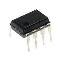
NCP1054P136 ON Semiconductor, NCP1054P136 Datasheet

NCP1054P136
Specifications of NCP1054P136
Related parts for NCP1054P136
NCP1054P136 Summary of contents
Page 1
NCP1050, NCP1051, NCP1052, NCP1053, NCP1054, NCP1055 Monolithic High Voltage Gated Oscillator Power Switching Regulator The NCP1050 through NCP1055 are monolithic high voltage regulators that enable end product equipment to be compliant with low standby power requirements. This device series combines ...
Page 2
AC Line Input Control Input Pin Function Description Pin Pin (SOT−223) (PDIP−8) Function Control Input Ground − Connection 3 5 Power Switch Drain ...
Page 3
AC Line Input Startup − Bypass/ 7.5/8 Fault Timing/ V Sweep CO Undervoltage Control Lockout − 4 ...
Page 4
OSC (high) 8 7.5 V Oscillator Duty Cycle Oscillator Clock 47 CONTROL, SINK 0 mA Leading Edge On Duty Cycle Off Power Switch Circuit Gate Drive Primary Current Figure 3. Timing Diagram ...
Page 5
I , Current Measurement CC1 V CC(on) Hysteretic Regulation V CC(off CC(reset 6 (start CC1 I CC2 CC3 (start) 47 ...
Page 6
MAXIMUM RATINGS Rating Power Switch and Startup Circuit Drain Voltage Range Drain Current Peak During Transformer Saturation Power Supply/V Bypass and Control Input CC Voltage Range Current Thermal Characteristics P Suffix, Plastic Package Case 626A−01 Junction−to−Lead Junction−to−Air, 2.0 Oz. Printed ...
Page 7
ELECTRICAL CHARACTERISTICS temperature range that applies (Note 1), unless otherwise noted.) Characteristics OSCILLATOR Frequency ( 25° kHz Version 100 kHz Version 136 kHz Version low high ...
Page 8
ELECTRICAL CHARACTERISTICS temperature range that applies (Note 2), unless otherwise noted.) Characteristics POWER SWITCH CIRCUIT Power Switch Circuit On−State Resistance NCP1050, NCP1051, NCP1052 ( mA 25° 125°C J NCP1053, NCP1054, NCP1055 (I ...
Page 9
ELECTRICAL CHARACTERISTICS temperature range that applies (Note 7), unless otherwise noted.) Characteristics TOTAL DEVICE Power Supply Current After UVLO Turn−On (Note 8) Power Switch Circuit Enabled NCP1050, NCP1051, NCP1052 44 kHz Version 100 kHz Version 136 kHz Version NCP1053, NCP1054, ...
Page 10
CC(on CC(off −50 − TEMPERATURE (°C) Figure 5. Oscillator Frequency (44 kHz Version) versus Temperature 142 CC(on) ...
Page 11
CURRENT RISING CURRENT FALLING 34 30 −50 − TEMPERATURE (°C) Figure 11. Upper Window Control Input Current Thresholds versus Temperature 4.66 4.64 4.62 4.60 I 4.58 SOURCE 4.56 4.54 4.52 −50 −25 ...
Page 12
TEMPERATURE (°C) Figure 17. Normalized Peak Current Limit versus Temperature 4.56 4.54 4.52 4.50 4.48 4.46 4.44 4.42 4.40 4.38 4.36 4.34 −50 − ...
Page 13
TEMPERATURE (°C) Figure 23. Supply Current versus Temperature (NCP1050/1/2) 0.48 0.47 0.46 0.45 0.44 0.43 0.42 0.41 −50 − ...
Page 14
Introduction The NCP105X series represents a new higher level of integration by providing on a single monolithic chip all of the active power, control, logic, and protection circuitry required to implement a high voltage flyback converter and compliance with very ...
Page 15
Current Limit Comparator and Power Switch Circuit The Power Switch Circuit is constructed with a SENSEFET™ in order to monitor the drain current. A portion of the current flowing through the circuit goes into a sense element The ...
Page 16
Two application examples have been provided in this document, and they are described in detail in this section. Figure 28 shows a Universal Input, 6 Watt Converter Application as well as a 5.5 Watt Charger Application using the NCP1053 @ ...
Page 17
Figure 28. Universal Input 6/5 Watt Converter/Charger Application http://onsemi.com 17 ...
Page 18
Test Line Regulation − 265 − 265 − 265 − 265 − 265 ...
Page 19
I = 120 mA out 5.220 I = 600 mA out 5.218 5.216 5.214 5.212 I = 1.2 A out 5.210 5.208 80 130 180 LINE INPUT VOLTAGE (V Figure 30. Converter Line Regulation ...
Page 20
LOAD CURRENT (A) Figure 36. Converter Efficiency Ch1: V out Ch2: Rectified 230 0.5 A) out Figure 38. Converter On/Off Line ...
Page 21
BOARD GRAPHICS AC Input − IC2 + L1 IC1 − Top View 2.75″ NCP1050 Series Bottom View Figure 40. Printed Circuit Board and Component Layout ...
Page 22
DEVICE ORDERING INFORMATION R DS(on) (W) Device NCP1050P44G 30 NCP1050P100G 30 NCP1050P136G 30 NCP1050ST44T3G 30 NCP1050ST100T3G 30 NCP1050ST136T3G 30 NCP1051P44G 30 NCP1051P100G 30 NCP1051P136G 30 NCP1051ST44T3G 30 NCP1051ST100T3G 30 NCP1051ST136T3G 30 NCP1052P44G 30 NCP1052P100G 30 NCP1052P136G 30 NCP1052ST44T3G 30 NCP1052ST100T3G ...
Page 23
... DEVICE ORDERING INFORMATION R DS(on) (W) Device NCP1054P44G 15 NCP1054P100G 15 NCP1054P136G 15 NCP1054ST44T3G 15 NCP1054ST100T3G 15 NCP1054ST136T3G 15 NCP1055P44G 15 NCP1055P100G 15 NCP1055P136G 15 NCP1055ST44T3G 15 NCP1055ST100T3G 15 NCP1055ST136T3G 15 †For information on tape and reel specifications, including part orientation and tape sizes, please refer to our Tape and Reel Packaging Spe- cifications Brochure, BRD8011/D. 9. Consult factory for additional optocoupler fail−safe latching, frequency, current limit and line input options. ...
Page 24
NOTE 3 C −T− N SEATING PLANE 0.13 (0.005) M PACKAGE DIMENSIONS PDIP−8 P SUFFIX CASE 626A−01 ISSUE http://onsemi.com 24 ...
Page 25
... A1 *For additional information on our Pb−Free strategy and soldering details, please download the ON Semiconductor Soldering and Mounting Techniques Reference Manual, SOLDERRM/D. SENSEFET is a trademark of Semiconductor Components Industries, LLC (SCILLC) ON Semiconductor and are registered trademarks of Semiconductor Components Industries, LLC (SCILLC). SCILLC reserves the right to make changes without further notice to any products herein ...


