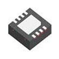
LM4991LDX National Semiconductor, LM4991LDX Datasheet

LM4991LDX
Specifications of LM4991LDX
Available stocks
Related parts for LM4991LDX
LM4991LDX Summary of contents
Page 1
... LM4991LD and LM4991M. Connection Diagrams Small Outline Package Top View Order Number LM4991MA See NS Package Number M08A Boomer ® registered trademark of National Semiconductor Corporation. © 2003 National Semiconductor Corporation Key Specifications n Improved PSRR at 217kHz and 1kHz 5.0V, 10% THD, 1kHz O DD LM4991LD (only), 3Ω ...
Page 2
Typical Application FIGURE 1. Typical Audio Amplifier Application Circuit www.national.com 2 20074001 ...
Page 3
... Absolute Maximum Ratings If Military/Aerospace specified devices are required, please contact the National Semiconductor Sales Office/ Distributors for availability and specifications. Supply Voltage Supply Temperature Input Voltage Power Dissipation (Note 4) ESD Susceptibility (Note 5) ESD Susceptibility (Note 6) Junction Temperature Electrical Characteristics V The following specifications apply for V ...
Page 4
Electrical Characteristics V The following specifications apply for V 25˚C. (Continued) Symbol Parameter PSRR Power Supply Rejection Ratio Electrical Characteristics V The following specifications apply for V Symbol Parameter Quiescent Power Supply I DD Current I Shutdown Current SD V ...
Page 5
External Components Description (Figure 1) Components 1. R Inverting input resistance that sets the closed-loop gain in conjunction with R i pass filter with Input coupling capacitor that blocks the DC voltage at the ...
Page 6
Typical Performance Characteristics THD+N vs Frequency 8Ω, and THD+N vs Frequency V = 2.6V 8Ω, and THD+N vs Output Power 4Ω, and ...
Page 7
Typical Performance Characteristics THD+N vs Output Power V = 2.6V 4Ω, and f = 1kHz DD L Power Supply Rejection Ratio (PSRR) vs Frequency 8Ω, input 10Ω terminated DD L Power Supply Rejection ...
Page 8
Typical Performance Characteristics Power Supply Rejection Ratio (PSRR) vs Frequency V = 2.6V 8Ω, input 10Ω terminated DD L Open Loop Frequency Response, 5V Power Dissipation vs Output Power www.national.com (Continued) Power Supply Rejection Ratio (PSRR) ...
Page 9
Typical Performance Characteristics Power Dissipation vs Output Power 2.6V DD Shutdown Hysteresis Voltage V = 3V, SD Mode = V DD Output Power vs Supply Voltage (Continued) 20074063 DD 20074073 = 4Ω 20074067 9 Shutdown Hysteresis ...
Page 10
Typical Performance Characteristics Output Power vs Supply Voltage, R Frequency Response vs Input Capacitor Size Application Information EXPOSED-DAP PACKAGE PCB MOUNTING CONSIDERATION The LM4991’s exposed-DAP (die attach paddle) package (LD) provides a low thermal resistance between the die and the ...
Page 11
Application Information LD (LLP) package is available from National Semiconduc- tor’s Package Engineering Group under application note AN1187. PCB LAYOUT AND SUPPLY REGULATION CONSIDERATIONS FOR DRIVING 3Ω AND 4Ω LOADS Power dissipated by a load is a function of the ...
Page 12
Application Information connected between the bypass pin and ground improves the internal bias voltage’s stability, producing improved PSRR. The improvements to PSRR increase as the bypass pin capacitor increases. Typical applications employ a 5V regu- lator with 10µF and a ...
Page 13
Application Information must make sure that the power supply choice along with the output impedance does not violate the conditions explained in the Power Dissipation section. Once the power dissipation equations have been addressed, the required differential gain can be ...
Page 14
Physical Dimensions www.national.com inches (millimeters) unless otherwise noted Order Number LM4991LD See NS Package Number LDC08A Order Number LM4991MA NS Package Number M08A 14 ...
Page 15
... NATIONAL’S PRODUCTS ARE NOT AUTHORIZED FOR USE AS CRITICAL COMPONENTS IN LIFE SUPPORT DEVICES OR SYSTEMS WITHOUT THE EXPRESS WRITTEN APPROVAL OF THE PRESIDENT AND GENERAL COUNSEL OF NATIONAL SEMICONDUCTOR CORPORATION. As used herein: 1. Life support devices or systems are devices or systems which, (a) are intended for surgical implant ...


