NVTFS5116PLTAG ON Semiconductor, NVTFS5116PLTAG Datasheet
NVTFS5116PLTAG
Manufacturer Part Number
NVTFS5116PLTAG
Description
MOSFET Power Single P-Channel 60V,14A,52mohm
Manufacturer
ON Semiconductor
Specifications of NVTFS5116PLTAG
Configuration
Single
Transistor Polarity
P-Channel
Resistance Drain-source Rds (on)
52 mOhms
Forward Transconductance Gfs (max / Min)
11 S
Drain-source Breakdown Voltage
- 60 V
Continuous Drain Current
- 14 A
Power Dissipation
21 W
Maximum Operating Temperature
+ 175 C
Mounting Style
SMD/SMT
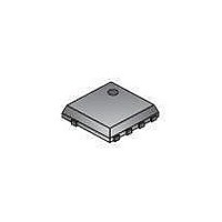
Package / Case
WDFN-8
Lead Free Status / Rohs Status
Details
Available stocks
Company
Part Number
Manufacturer
Quantity
Price
Company:

Part Number:
NVTFS5116PLTAG
Manufacturer:
ON Semiconductor
Quantity:
1 200
Part Number:
NVTFS5116PLTAG
Manufacturer:
ON/安森美
Quantity:
20 000
Company:
Part Number:
NVTFS5116PLTAG
Manufacturer:
ON
Quantity:
8 533
Company:
Part Number:
NVTFS5116PLTAG
Manufacturer:
ON
Quantity:
15 364


NVTFS5116PL
Power MOSFET
−60 V, −14 A, 52 mW, Single P−Channel
Features
•
•
•
•
•
Stresses exceeding Maximum Ratings may damage the device. Maximum
Ratings are stress ratings only. Functional operation above the Recommended
Operating Conditions is not implied. Extended exposure to stresses above the
Recommended Operating Conditions may affect device reliability.
1. The entire application environment impacts the thermal resistance values shown,
2. Psi (Y) is used as required per JESD51−12 for packages in which
3. Surface−mounted on FR4 board using a 650 mm
4. Continuous DC current rating. Maximum current for pulses as long as 1
MAXIMUM RATINGS
© Semiconductor Components Industries, LLC, 2011
January, 2011 − Rev. 0
THERMAL RESISTANCE MAXIMUM RATINGS
Drain−to−Source Voltage
Gate−to−Source Voltage
Continuous Drain Cur-
rent R
2, 3, 4)
Power Dissipation
R
Continuous Drain Cur-
rent R
3, 4)
Power Dissipation
R
Pulsed Drain Current
Operating Junction and Storage Temperature
Source Current (Body Diode)
Single Pulse Drain−to−Source Avalanche
Energy (T
I
Lead Temperature for Soldering Purposes
(1/8″ from case for 10 s)
Junction−to−Mounting Board (top) − Steady
State (Note 2 and 3)
Junction−to−Ambient − Steady State (Note 3)
L(pk)
AEC−Q101 Qualified Site and Change Controls
Small Footprint (3.3 x 3.3 mm) for Compact Design
Low R
Low Capacitance to Minimize Driver Losses
NV Prefix for Automotive and Other Applications Requiring
These are Pb−Free Devices
YJ−mb
qJA
they are not constants and are only valid for the particular conditions noted.
substantially less than 100% of the heat flows to single case surface.
second is higher but is dependent on pulse duration and duty cycle.
(Notes 1, 3)
= 30 A, L = 0.1 mH, R
YJ−mb
qJA
(Notes 1, 2, 3)
DS(on)
(Notes 1 &
J
= 25°C, V
(Notes 1,
to Minimize Conduction Losses
Parameter
Parameter
DD
(T
= 50 V, V
Steady
Steady
T
J
State
State
A
G
= 25°C unless otherwise noted)
= 25°C, t
= 25 W)
GS
T
T
T
T
T
T
mb
mb
T
T
mb
mb
A
A
= 10 V,
A
A
p
= 100°C
= 100°C
= 25°C
= 25°C
= 100°C
= 100°C
= 10 ms
= 25°C
= 25°C
Symbol
R
Symbol
T
2
R
V
YJ−mb
, 2 oz. Cu pad.
J
V
E
I
P
P
, T
DSS
DM
T
qJA
I
I
I
GS
AS
D
D
S
D
D
L
(Note 1)
stg
Value
−55 to
Value
−126
+175
7.2
−60
±20
−14
−10
−17
260
47
3.2
1.6
21
10
−6
−4
45
1
°C/W
Unit
Unit
mJ
°C
°C
W
W
V
V
A
A
A
A
NVTFS5116PLTAG
NVTFS5116PLTWG
†For information on tape and reel specifications,
including part orientation and tape sizes, please
refer to our Tape and Reel Packaging Specification
Brochure, BRD8011/D.
V
CASE 511AB
(BR)DSS
−60 V
(Note: Microdot may be in either location)
Device
WDFN8
(m8FL)
ORDERING INFORMATION
5116
A
Y
WW
G
G (4)
1
http://onsemi.com
P−Channel MOSFET
72 mW @ −4.5 V
52 mW @ −10 V
R
= Specific Device Code
= Assembly Location
= Year
= Work Week
= Pb−Free Package
D (5−8)
DS(on)
(Pb−Free)
(Pb−Free)
Package
WDFN8
WDFN8
MARKING DIAGRAM
Publication Order Number:
G
S
S
S
MAX
1
S (1,2,3)
AYWWG
1500/Tape & Reel
5000/Tape & Reel
5116
NVTFS5116PL/D
G
Shipping
I
D
−14 A
MAX
D
D
D
D
†
Related parts for NVTFS5116PLTAG
Image
Part Number
Description
Manufacturer
Datasheet
Request
R

Part Number:
Description:
ON Semiconductor [VOLTAGE REGULATOR]
Manufacturer:
ON Semiconductor
Datasheet:
Part Number:
Description:
357-036-542-201 CARDEDGE 36POS DL .156 BLK LOPRO
Manufacturer:
ON Semiconductor
Datasheet:
Part Number:
Description:
357-036-542-201 CARDEDGE 36POS DL .156 BLK LOPRO
Manufacturer:
ON Semiconductor
Datasheet:
Part Number:
Description:
357-036-542-201 CARDEDGE 36POS DL .156 BLK LOPRO
Manufacturer:
ON Semiconductor
Datasheet:
Part Number:
Description:
357-036-542-201 CARDEDGE 36POS DL .156 BLK LOPRO
Manufacturer:
ON Semiconductor
Datasheet:
Part Number:
Description:
357-036-542-201 CARDEDGE 36POS DL .156 BLK LOPRO
Manufacturer:
ON Semiconductor
Datasheet:
Part Number:
Description:
357-036-542-201 CARDEDGE 36POS DL .156 BLK LOPRO
Manufacturer:
ON Semiconductor
Datasheet:
Part Number:
Description:
357-036-542-201 CARDEDGE 36POS DL .156 BLK LOPRO
Manufacturer:
ON Semiconductor
Datasheet:
Part Number:
Description:
357-036-542-201 CARDEDGE 36POS DL .156 BLK LOPRO
Manufacturer:
ON Semiconductor
Datasheet:
Part Number:
Description:
357-036-542-201 CARDEDGE 36POS DL .156 BLK LOPRO
Manufacturer:
ON Semiconductor
Datasheet:
Part Number:
Description:
357-036-542-201 CARDEDGE 36POS DL .156 BLK LOPRO
Manufacturer:
ON Semiconductor
Datasheet:
Part Number:
Description:
Manufacturer:
ON Semiconductor
Datasheet:
Part Number:
Description:
Manufacturer:
ON Semiconductor
Datasheet:
Part Number:
Description:
Manufacturer:
ON Semiconductor
Datasheet: