AD8016ARE-REEL7 Analog Devices Inc, AD8016ARE-REEL7 Datasheet
AD8016ARE-REEL7
Specifications of AD8016ARE-REEL7


Related parts for AD8016ARE-REEL7


AD8016ARE-REEL7 Summary of contents
Page 1
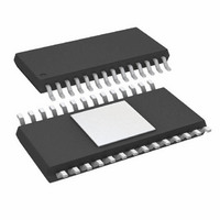
... NC AGND 8 13 PWDN1 PWDN0 9 12 BIAS DGND 10 –V2 11 – CONNECT 28-Lead TSSOP-EP (RE-28- – PWDN1 BIAS 6 23 OUT 22 –V2 +V2 7 AD8016ARE –V1 + DGND 9 OUT – PWDN0 CONNECT www.analog.com © 2003 Analog Devices, Inc. All rights reserved OUT INN INP AGND 20 AGND ...
Page 2
AD8016–SPECIFICATIONS Parameter DYNAMIC PERFORMANCE –3 dB Bandwidth Bandwidth for 0.1 dB Flatness Large Signal Bandwidth Peaking Slew Rate Rise and Fall Time Settling Time Input Overdrive Recovery Time NOISE/DISTORTION PERFORMANCE Distortion, Single-Ended Second Harmonic Third Harmonic Multitone Power Ratio* IMD ...
Page 3
C, V SPECIFICATIONS T MAX Parameter DYNAMIC PERFORMANCE –3 dB Bandwidth Bandwidth for 0.1 dB Flatness Large Signal Bandwidth Peaking Slew Rate Rise and Fall Time Settling Time Input Overdrive Recovery Time NOISE/DISTORTION PERFORMANCE Distortion, Single-Ended Second Harmonic ...
Page 4
... AD8016ARB AD8016ARB-REEL AD8016ARB-EVAL AD8016ARE AD8016ARE-REEL AD8016ARE-REEL7 AD8016ARE-EVAL CAUTION ESD (electrostatic discharge) sensitive device. Electrostatic charges as high as 4000 V readily accumulate on the human body and test equipment and can discharge without detection. Although the AD8016 features proprietary ESD protection circuitry, permanent damage may occur on devices subjected to high energy electrostatic discharges ...
Page 5
V IN 49.9 0.1 F 0.1 F Figure 3. Single-Ended Test Circuit 100mV OUT V = 20mV IN TIME (100ns/DIV) Figure 4. 100 mV Step Response + Ω ...
Page 6
AD8016 – 499 F – + p-p O –50 –60 –70 –80 –90 –100 –110 0.01 0.1 1 FREQUENCY (MHz) Figure 9. Distortion vs. Frequency; Second Harmonic, = ± ...
Page 7
R = 499 F – –40 –45 (0,0) –50 (0,1) –55 –60 –65 –70 –75 –80 0 100 200 300 PEAK OUTPUT CURRENT (mA) Figure 15. Distortion vs. Peak Output Current; Second = ± ...
Page 8
AD8016 3 0 – 40mV p-p IN – 100 –9 L –12 –15 –18 –21 –24 – FREQUENCY (MHz) Figure 21. Frequency Response PWDN1, PWDN0 Codes ...
Page 9
NOISE NOISE 100 1k 10k FREQUENCY (MHz) Figure 27. Noise vs. Frequency +2mV (–0.1%) 0 –2mV (–0.1 OUT V OUT – ...
Page 10
AD8016 V OUT –100 0 100 200 300 400 500 TIME (ns) Figure 33a. Overload Recovery 100 Ω + OUT –100 0 100 200 300 ...
Page 11
THEORY OF OPERATION The AD8016 is a current feedback amplifier with high (500 mA) output current capability. With a current feedback amplifier, the current into the inverting input is the feedback signal and the open-loop behavior is that of a ...
Page 12
AD8016 BIAS pin (I ) and the supply current (I BIAS down I is less than 1 mA total. Alternatively, an external pull- Q down resistor to ground or a current sink attached to the BIAS pin can be used ...
Page 13
... WFM files can be obtained through the Analog Devices website, at www.analog.com. EVALUATION BOARDS The AD8016ARP-EVAL, AD8016ARB-EVAL, AD8016ARE- EVAL boards available through Analog Devices provide a platform for evaluating the AD8016 in an ADSL differential line driver circuit. The board is laid out to accommodate Analog Devices’ ...
Page 14
... Testing was conducted using a 1 oz. copper board in an ambient temperature of ~24°C over air flows of 200, 150, 100, and 50 (0.200 and 400 for AD8016ARE) linear feet per minute (LFM) and for ARP and ARB packages as well as in still air. The 4-layer PCB was designed to maximize the ...
Page 15
... LFM of air flow. Note that the AD8016ARE is targeted at xDSL applications other than full-rate CO ADSL. The AD8016ARE is targeted at g.lite and other xDSL applications where reduced power dissi- pation can be achieved through a reduction in output power. ...
Page 16
AD8016 Figure 45. DMT Signal Generator Schematic –16– REV. B ...
Page 17
TP10 TP5 AGND3,4 R11 R13 JP6 R23 1 JP5 AGND3,4,5 R14 S6 R16 R15 C10 TP11 TP4 ...
Page 18
AD8016 LAYOUT AD8016ARB-EVAL Figure 47. Assembly Figure 48. Layer 1 Figure 49. Power/Ground Plane Figure 50. Layer 1 Figure 51. Silkscreen Bottom –18– REV. B ...
Page 19
ALP – EVALUATION BOARD – BILL OF MATERIALS Quantity Description 10 µ Size Tantalum Chip Capacitor 5 0.1 µ 1206 Size Ceramic Chip Capacitor 10 49.9 Ω 1% 1/8 W 1206 Size Chip Resistor 2 100 ...
Page 20
AD8016 20-Lead Power SOIC, Thermally Enhanced Package [PSOP3] 11.00 BSC 3.60 3.35 3.10 SEATING PLANE 28-Lead Thin Shrink Small Outline With Exposed Pad [TSSOP-EP PIN 1 1.20 MAX 0.15 0.00 Revision History Location 11/03—Data Sheet changed from REV. ...