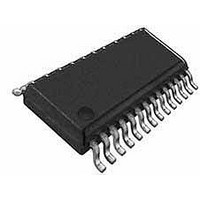
ST62T65CN6 STMicroelectronics, ST62T65CN6 Datasheet - Page 68

ST62T65CN6
Manufacturer Part Number
ST62T65CN6
Description
Microcontrollers (MCU) OTP EPROM 4K SPI
Manufacturer
STMicroelectronics
Datasheet
1.ST62T55CM6.pdf
(86 pages)
Specifications of ST62T65CN6
Processor Series
ST62T6x
Core
ST6
Data Bus Width
8 bit
Program Memory Type
EPROM
Program Memory Size
3884 B
Data Ram Size
128 B
Interface Type
SCI
Maximum Clock Frequency
8 MHz
Number Of Programmable I/os
21
Number Of Timers
1
Operating Supply Voltage
3 V to 6 V
Maximum Operating Temperature
+ 125 C
Mounting Style
SMD/SMT
Package / Case
SSOP-28
Minimum Operating Temperature
- 40 C
On-chip Adc
8 bit
Lead Free Status / Rohs Status
Details
Available stocks
Company
Part Number
Manufacturer
Quantity
Price
Company:
Part Number:
ST62T65CN6
Manufacturer:
SEK
Quantity:
1 000
Part Number:
ST62T65CN6
Manufacturer:
ST
Quantity:
20 000
ST62T55C ST62T65C/E65C
DC ELECTRICAL CHARACTERISTICS (Cont’d)
(T
Note:
(*) All Peripherals in stand-by.
6.4 AC ELECTRICAL CHARACTERISTICS
(T
Notes:
1. Period for which V
2 An oscillator frequency above 1MHz is recommended for reliable A/D results.
3. Measure performed with OSCin pin soldered on PCB, with an around 2pF equivalent capacitance.
68/86
Endurance
Retention EEPROM Data Retention
Symbol
Symbol
A
A
T
C
f
f
V
t
V
LFAO
V
V
I
OSG
C
REC
f
= -40 to +85°C unless otherwise specified))
= -40 to +125°C unless otherwise specified)
WEE
DD
(2)
OUT
RC
OH
OL
up
dn
IN
LVD Threshold in power-on
LVD threshold in powerdown
Low Level Output Voltage
All Output pins
Low Level Output Voltage
30 mA Sink I/O pins
High Level Output Voltage
All Output pins
Supply Current in STOP
Mode, with LVD disabled
Supply Recovery Time
EEPROM Write Time
EEPROM WRITE/ERASE Cycle
Internal frequency with LFAO active
Internal Frequency with OSG
enabled
Internal frequency with RC oscilla-
tor and OSG disabled
Input Capacitance
Output Capacitance
DD
has to be connected at 0V to allow internal Reset function at next power-up.
2)
Parameter
Parameter
2) 3)
(1)
(*)
V
V
V
V
V
V
V
V
V
I
V
LOAD
DD
DD
DD
DD
DD
DD
DD
DD
DD
DD
= 5.0V; I
= 5.0V; I
= 5.0V; I
= 5.0V; I
= 5.0V; I
= 5.0V; I
= 5.0V; I
= 5.0V; I
= 5.0V; I
=5.0V
=0mA
T
T
T
Q
T
V
V
V
V
VDD=5.0V (Except 626xB ROM)
R=47k
R=100k
R=470k
VDD=5.0V (626xB ROM)
R=10k
R=27k
R=67k
R=100k
All Inputs Pins
All Outputs Pins
Test Conditions
A
A
A
A
DD
DD
DD
DD
A
= 25°C
= 85°C
= 125°C
= 55°C
L
OT
= 3V
= 3.6V
= 4.5V
= 6V
OL
OL
OL
OL
OL
OL
OL
OH
OH
Acceptance (25°C)
= +10µA
= + 5mA
= + 10mAv
= +10µA
= +10mA
= +20mA
= +30mA
Test Conditions
= -10µA
= -5.0mA
V
dn
Min.
+50 mV
3.6
4.9
3.5
300,000 1 million
Min.
100
200
800
2.7
6.3
4.7
2.8
2.2
10
1
1
2
2
4
Value
Typ.
4.1
3.8
Value
Typ.
400
850
3.2
8.2
5.9
3.6
2.8
10
20
5
5
V
up
Max.
4.3
-50 mV
0.1
0.8
1.2
0.1
0.8
1.3
2.0
10
Max.
f
800
900
OSC
5.8
3.5
9.8
4.3
3.4
10
20
30
10
10
7
Unit
cycles
years
MHz
MHz
MHz
MHz
MHz
MHz
MHz
V
V
V
V
Unit
kHz
kHz
ms
ms
A
pF
pF


