STA515W STMicroelectronics, STA515W Datasheet
STA515W
Specifications of STA515W
Available stocks


Related parts for STA515W


STA515W Summary of contents
Page 1
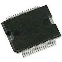
... THD at V or, in single parallel BTL configuration into a 8-Ω load with 10% THD at V The input pins have a threshold proportional to the voltage on pin VL. The STA515W comes in a 36-pin PowerSSO package with exposed pad down (EPD). Package PowerSSO36 EPD PowerSSO36 EPD ...
Page 2
... Introduction 1 Introduction Figure 1. STA515W circuit for quad single-ended amplifiers IN1A +3.3V CONFIG PWR_DN PWRDN R57 R59 10K 10K TRISTATE C58 100nF THWARN TH_WARN IN1B C58 C53 100nF VCCSIG 100nF C60 VCCSIG 100nF IN2A GNDREG GNDCLEAN IN2B GNDSUB 2/14 VCC1A 15 IN1A 29 M3 ...
Page 3
... VCC1B 13 GND1B 14 GND1A 15 VCC1A 16, 17 OUT1A 18 N.C. 19 GNDCLEAN 20 GNDREG 21, 22 VDD 23 VL GNDSUB 1 OUT2B 2 OUT2B 3 VCC2B 4 GND2B 5 GND2A 6 STA515W VCC2A 7 OUT2A 8 OUT2A 9 OUT1B 10 OUT1B 11 VCC1B 12 GND1B 13 GND1A 14 15 VCC1A 16 OUT1A 17 OUT1A 18 N.C. Type PWR Substrate ground O Output half bridge 2B PWR Positive supply ...
Page 4
... Thermal-warning advisor (open-drain device, needs pull-up resistor temperature of the IC >130 1: normal operation I Input of half bridge 1A I Input of half bridge 1B I Input of half bridge 2A I Input of half bridge 2B PWR 5-V regulator referred to +V PWR Signal positive supply Doc ID 11079 Rev 2 STA515W Description Parallel-output and high-current ...
Page 5
... STA515W 3 Electrical characteristics Table 3. Absolute maximum ratings Symbol V DC supply voltage (Pins 4, 7, 12, 15 Maximum voltage on pins max T Operating temperature range op P Power dissipation (Tcase = 70 °C) tot Storage and junction temperature stg j Table 4. Recommended operating conditions Symbol V DC supply voltage (Pins 4, 7, 12, 15) ...
Page 6
... Resistive load see Figure 3 Resistive load see Figure PWRDN V = 3.3 V pin TRISTATE Input pulse width = 50% duty switching frequency = 384 kHz filters - - No load Doc ID 11079 Rev 2 Min Typ Max = 3 100 - - 100 - - 300 300 0.8 1 150 STA515W Unit µA µA µ ...
Page 7
... STA515W Table 7. Threshold switching voltage variation with voltage on pin VL Voltage on pin VL, V 2.7 3.3 5.0 Table 8. Logic truth table Inputs as per Pin TRISTATE INxA Test circuits Figure 3. Test circuit Figure 4. Current dead time test circuit Duty cycle=A DTin(A) INA V max L LOW ...
Page 8
... Applications information 4 Applications information The STA515W is a dual channel H-bridge that can deliver 20 W per channel into 8 Ω with 10% THD The STA515W converts both DDX and binary-logic-controlled PWM signals into audio power at the load. It includes a logic interface, integrated bridge drivers, high efficiency MOSFET outputs and thermal and short-circuit protection circuitry ...
Page 9
... INLA = INLB and INRA = INRB, then the corresponding outputs can be shorted together to give OUTLA = OUTLB and OUTRA = OUTRB. Output filter A passive 2nd-order filter is used on the STA515W power outputs to reconstruct an analog audio signal. The system performance can be significantly affected by the output filter design and choice of passive components. ...
Page 10
... C60 100nF IN2A GNDCLEAN IN2B Figure 8 below shows a single-BTL configuration capable of supplying 40 W into a 4-Ω load at 10% THD with V STA308+STA515W+STA50X demo board. A PWM modulator as driver is required. Figure 8. Typical single-BTL configuration for 40 W +3.3V 100nF 100nF 10K X7R TH_WARN nPWR_DN ...
Page 11
... STA515W 5 Package mechanical data The STA515W comes in a 36-pin PowerSSO package with exposed pad down (EPD). Figure 9 below shows the package outline and In order to meet environmental requirements, ST offers these devices in different grades of ® ECOPACK packages, depending on their level of environmental compliance. ECOPACK specifications, grade definitions and product status are available at: www.st.com. ® ...
Page 12
Figure 9. PowerSSO36 EPD outline drawing h x 45° ...
Page 13
... STA515W 6 Revision history Table 10. Document revision history Date Nov-2004 27-Apr-2010 Revision 1 Initial release. Added order code STA515W13TR Modified Figure 1 on page 2 Reconstructed pin list in former table 3 Functional pin status 2 Updated Vlow and Vhigh spec in Modified Figure 3 and Updated applications circuits in Doc ID 11079 Rev 2 ...
Page 14
... Australia - Belgium - Brazil - Canada - China - Czech Republic - Finland - France - Germany - Hong Kong - India - Israel - Italy - Japan - Malaysia - Malta - Morocco - Philippines - Singapore - Spain - Sweden - Switzerland - United Kingdom - United States of America 14/14 Please Read Carefully: © 2010 STMicroelectronics - All rights reserved STMicroelectronics group of companies www.st.com Doc ID 11079 Rev 2 STA515W ...