STA533WF STMicroelectronics, STA533WF Datasheet
STA533WF
Specifications of STA533WF
Available stocks


Related parts for STA533WF


STA533WF Summary of contents
Page 1
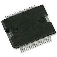
... THD at V or, in single parallel BTL configuration into a 4-Ω load with 10% THD at V The input pins have a threshold proportional to the voltage on pin VL. The STA533WF comes in a 36-pin PowerSSO package with exposed pad down (EPD). Temperature range PowerSSO36 EPD PowerSSO36 EPD ...
Page 2
... Output half bridge internal connection PWR Logical ground Filtering for regulator; this is an internally generated ground for PWR V DD PWR 5-V regulator referred to ground PWR High logical state setting voltage, V Doc ID 17658 Rev 1 STA533WF 36 VCCSIG 35 VCCSIG 34 VSS 33 VSS 32 IN2B 31 IN2A 30 IN1B ...
Page 3
... STA533WF Table 2. Pin list (continued) Pin Name 24 CONFIG 25 PWRDN 26 TRISTATE 27 FAULT 28 THWARN 29 IN1A 30 IN1B 31 IN2A 32 IN2B 33, 34 VSS 35, 36 VCCSIG Type Configuration pin: 0: normal operation I 1: bridges in parallel, see operation on page 8 Stand-by pin low-power mode 1: normal operation Hi-Z pin all power amplifier outputs in high-impedance state ...
Page 4
... Dt_s Low current dead time (static) 4/15 Parameter Parameter Parameter Table °C. amb Parameter Test conditions THD+N > 10 dsON dsON see Figure 2 Doc ID 17658 Rev 1 STA533WF Value 23 4.0 -0 0 0.3 DD -40 to 150 Min Typ Max 5 2.7 3.3 3 Min Typ Max - - 1 ...
Page 5
... STA533WF Table 6. Electrical characteristics (continued) Symbol High current dead time Dt_d (dynamic) t Turn-on delay time d_ON t Turn-off delay time d OFF t Rise time r t Fall time f Half-bridge input, low-level V IN-Low voltage Half-bridge input, high-level V IN-High voltage I High-level input current IN-H I Low-level input current ...
Page 6
... High Current Dead time for Bridge application = ABS(DTout(A)-DTin(A))+ABS(DTOUT(B)-DTin(B DTout(A) Q1 Rload=8Ω OUTxA 22µ Iout Q3 470nF 470nF Duty cycle A and B: Fixed to have DC output current of Iout in the direction shown in figure Doc ID 17658 Rev 1 STA533WF Figure 3 Output mode Off Off Off Hi Z Off On On Dump ...
Page 7
... STA533WF 3 Applications information The STA533WF is a dual-channel H-bridge audio power amplifier that can deliver 20 W per channel into 8 Ω with 10% THD at V The STA533WF converts both FFX and binary-logic-controlled PWM signals into audio power at the load. It includes a logic interface, integrated bridge drivers, high-efficiency MOSFET outputs and thermal and short-circuit protection circuitry ...
Page 8
... VL has settled. Parallel-output and high-current operation When using FFX mode, the STA533WF outputs can be connected in parallel to increase the output current capability. In this configuration the device can provide 40 W into 4 Ω. This mode of operation is enabled with pin CONFIG connected to V combined to give INLA = INLB and INRA = INRB, then the corresponding outputs can be shorted together to give OUTLA = OUTLB and OUTRA = OUTRB ...
Page 9
... Pin VCCSIG is used to filter the internal reference voltage V connected to other supply pins internally generated supply. Output filter A passive 2nd-order filter is used on the STA533WF power outputs to reconstruct an analog audio signal. The system performance can be significantly affected by the output filter design and choice of passive components. ...
Page 10
... INPUT_B 29 IN1A THWARN 27 FAULT R5 10k 26 TRISTATE EAPD 25 PWRDN 24 CONFIG 3V3 C12 VDD 100nF C13 C14 21 VDD 20 GNDREG 100nF 100nF 19 GNDCLEAN C18 STA533WF 100nF L3 22uH C20 100nF C23 100nF 22 6 C25 1uF 25V C26 R9 6 6.2 7 330pF 8 9 C28 22uH 100nF 12 13 ...
Page 11
... STA533WF 4 Heatsink requirements Using the STA533WF mounted on a double-layer PCB having 2 copper ground areas and with 16 via holes the junction to ambient thermal resistance is approximately 24 °C/W in natural air convection. Figure 8. Double-layer PCB with copper ground areas and 16 via holes With the dissipated power within the device depending primarily on the supply voltage, the ...
Page 12
... Package mechanical data 5 Package mechanical data The STA533WF comes in a 36-pin PowerSSO package with exposed pad down (EPD). Figure 10 below shows the package outline and In order to meet environmental requirements, ST offers these devices in different grades of ® ECOPACK packages, depending on their level of environmental compliance. ECOPACK specifications, grade definitions and product status are available at: www.st.com. ® ...
Page 13
Figure 10. PowerSSO36 EPD outline drawing h x 45° ...
Page 14
... Revision history 6 Revision history Table 9. Document revision history Date 02-Jul-2010 14/15 Revision 1 Initial release. Doc ID 17658 Rev 1 STA533WF Changes ...
Page 15
... STA533WF Information in this document is provided solely in connection with ST products. STMicroelectronics NV and its subsidiaries (“ST”) reserve the right to make changes, corrections, modifications or improvements, to this document, and the products and services described herein at any time, without notice. All ST products are sold pursuant to ST’s terms and conditions of sale. ...