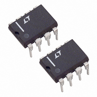
LTC1063CN8 Linear Technology, LTC1063CN8 Datasheet

LTC1063CN8
Specifications of LTC1063CN8
Available stocks
Related parts for LTC1063CN8
LTC1063CN8 Summary of contents
Page 1
... Low Level Filtering ■ Digital Voltmeters ■ 60Hz Lowpass Filters ■ Smoothing Filters ■ Reconstruction Filters , LTC and LT are registered trademarks of Linear Technology Corporation. All other trademarks are the property of their respective owners. U TYPICAL APPLICATIO 2.5kHz 5th Order Lowpass Filter ...
Page 2
... U RATINGS (Note 1) Operating Temperature Range ............... – 40°C to 85°C Storage Temperature Range ................ – 65°C to 150°C ≤ Lead Temperature (Soldering, 10 sec)................. 300°C + 0.3V ORDER PART NUMBER LTC1063CN8 GND – CLK OUT 8 LTC1063CJ8 LTC1063MJ8 16-LEAD PLASTIC SO WIDE T JMAX The ● ...
Page 3
ELECTRICAL CHARACTERISTICS temperature range, otherwise specifications are at V PARAMETER CONDITIONS Filter Gain V ±2.375 ≤ V Clock Feedthrough ±2.375 ≤ V Wideband Noise (Note 4) THD + Wideband Noise (Note Filter Output ± DC Swing V ...
Page 4
LTC1063 ELECTRICAL CHARACTERISTICS temperature range, otherwise specifications are at V PARAMETER CONDITIONS Power Supply Current Note 1: Absolute Maximum Ratings are those values beyond which the life of a device may be impaired. Note 2: The maximum ...
Page 5
W U TYPICAL PERFOR A CE CHARACTERISTICS = ±2.5V Gain vs Frequency –10 –20 – –40 – 0.5MHz CLK 1MHz CLK – 2MHz CLK ...
Page 6
LTC1063 W U TYPICAL PERFOR A CE CHARACTERISTICS Passband Gain and Phase vs Input Frequency 1 ±2.5V ≤ V ≤ ±7.5V 25° – –2 PHASE PHASE –3 –4 f =100kHz CLK –5 ...
Page 7
CTIO S Power Supply Pins (Pins Package) The positive and negative supply pin should be bypassed with a high quality 0.1µF ceramic capacitor. In applications where the clock pin (5) is externally ...
Page 8
LTC1063 CTIO S Output Pin (Pin 7, N Package) Pin 7 is the filter output. This pin can typically source over 20mA and sink 2mA. Pin 7 should not drive long coax cables, otherwise the ...
Page 9
U U APPLICATIO S I FOR ATIO Self-Clocking Operation The LTC1063 features an internal oscillator which can be tuned via an external RC. The LTC1063’s internal oscillator is primarily intended for generation of clock frequencies below 500kHz. The first curve ...
Page 10
LTC1063 U U APPLICATIO S I FOR ATIO 0.80 0.75 0.70 0.65 0.60 = ±7. 0. 0.50 0.45 = ±2. 0.40 0.5 1.0 1.5 2.0 CLOCK FREQUENCY (MHz) Figure CLK ...
Page 11
U U APPLICATIO S I FOR ATIO noise ratio at a given distortion level. The wideband noise (µ nearly independent of the value of the clock RMS frequency and excludes the clock feedthrough. The LTC1063’s typical wideband noise ...
Page 12
LTC1063 U U APPLICATIO S I FOR ATIO Group Delay The group delay of the LTC1063 closely approximates the delay of an ideal 5-pole Butterworth lowpass filter (Figure 11, Curve A). To linearize the group delay of the LTC1063 (Figure ...
Page 13
PACKAGE DESCRIPTIO CORNER LEADS OPTION .045 – .068 (1.143 – 1.650) FULL LEAD OPTION .300 BSC (7.62 BSC) .008 – .018 (0.203 – 0.457) NOTE: LEAD DIMENSIONS APPLY TO SOLDER DIP/PLATE OR TIN PLATE LEADS U J8 Package 8-Lead CERDIP ...
Page 14
LTC1063 PACKAGE DESCRIPTIO .300 – .325 (7.620 – 8.255) .008 – .015 (0.203 – 0.381) +.035 .325 –.015 ( ) +0.889 8.255 –0.381 NOTE: INCHES 1. DIMENSIONS ARE MILLIMETERS *THESE DIMENSIONS DO NOT INCLUDE MOLD FLASH OR PROTRUSIONS. MOLD FLASH ...
Page 15
... MOLD FLASH OR PROTRUSIONS SHALL NOT EXCEED .006" (0.15mm) Information furnished by Linear Technology Corporation is believed to be accurate and reliable. However, no responsibility is assumed for its use. Linear Technology Corporation makes no represen- tation that the interconnection of its circuits as described herein will not infringe on existing patent rights. ...
Page 16
... Noise 100kHz-10MHz 3V Supply RMS 86µV Noise 100kHz-20MHz 3V Supply RMS www.linear.com ● 81Hz 465 590 715 840 965 1090 1215 1340 1465 INPUT FREQUENCY (Hz) < 64kHz C < 300kHz C LT/LT 0905 REV A • PRINTED IN USA © LINEAR TECHNOLOGY CORPORATION 1993 1063 TA07 1063fa ...


