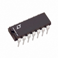
LTC1064-3CN Linear Technology, LTC1064-3CN Datasheet

LTC1064-3CN
Specifications of LTC1064-3CN
Available stocks
Related parts for LTC1064-3CN
LTC1064-3CN Summary of contents
Page 1
... In fact the LTC1064-3 overall performance competes with equivalent multiple op amp RC active realizations. The LTC1064-3 is available in a 14-pin DIP or 16-pin surface mounted SOL package. The LTC1064-3 is fabricated using LTC’s enhanced analog CMOS Si-gate process. The LTC1064-3 is pin compatible with the LTC1064-1, LTC1064-2 and LTC1064-4 ...
Page 2
... S Total Harmonic Distortion Wideband Noise (Note 1) Operating Temperature Range LTC1064-3M (OBSOLETE) ............... – 55°C to 125°C LTC1064-3C ....................................... – 40°C to 85°C Input Voltage ........................... (V Burn-In Voltage ....................................................... 15V W U ORDER PART NUMBER 1 NC LTC1064-3CN AGND + AGND 16-LEAD PLASTIC (WIDE) SO LTC1064-3MJ T JMAX LTC1064-3CJ The denotes the specifications which apply over the full operating = 25° ...
Page 3
... V = ±7. 25° CLK f –3dB 90 135 180 225 270 315 360 405 450 FREQUENCY (kHz) LTC1064-3 = 2MHz 10k, TTL or CMOS clock input level CLK MIN TYP ± 30 ± 20 ± 3/1 200 ±2.37 Group Delay 110 100 = 750kHz 90 = 10kHz 750kHz 10kHz CLK – ...
Page 4
... LTC1064 TYPICAL PERFOR A CE CHARACTERISTICS Phase Matching 2 ±7. 1.5MHz CLK f = 20kHz –3dB 1.8 50 UNIT SAMPLE (T = 25°C TO 125°C) A 1.6 1.4 1.2 1.0 0.8 0.6 0.4 0 FREQUENCY (kHz) 1064 G04 Table 1. Wideband Noise (µV Pin – V GND 4 Total Harmonic Distortion 1 ...
Page 5
... LTC1064-3 = 1kHz, LTC1064-3 Typical Response –3dB + = 75kHz, Pin (fltr 75:1) CLK GAIN (dB) DELAY (ms) – 0.281 0.502 – 0.420 0.503 – 0.610 0.503 – 0.860 0.502 – 1.160 0.502 – ...
Page 6
... LTC1064-3 Typical Response –3dB = 120kHz, Pin 10 at GND (fltr 120:1) CLK GAIN (dB) DELAY (ms) –0.354 0.458 –0.520 0.456 –0.730 0.454 –1.000 0.452 –1.320 0.449 –1.670 0.448 – ...
Page 7
... For ±7V sup- plies and above, the maximum clock frequency is 7MHz. Do not allow the clock levels to exceed the power supplies. For single supply operation ≥6V use level shifting at Pin 11 2 with T L levels (see Figure 4). LTC1064 120:1 when – . This pin + or V (Figure 1) ...
Page 8
... V f CLK 0.1µ – AGND 75/150 10k OUT 0.1µ INV A NC RECOMMENDED OP AMPS: LT1022, LT318, LT1056 Figure 1. Buffering the Filter Output. The Buffer Op Amp Should Not Share the LTC1064-3 Power Lines LTC1064-3 3 AGND 15V V 0.1µF 5 AGND 0.1µF ...
Page 9
... RAD TYP 0° – 15° .045 – .065 (1.143 – 1.651) .014 – .026 (0.360 – 0.660) OBSOLETE PACKAGE LTC1064 .220 – .310 (5.588 – 7.874 .200 (5.080) MAX .015 – .060 (0.381 – 1.524) .100 .125 (2.54) (3.175) ...
Page 10
... LTC1064-3 PACKAGE DESCRIPTIO .300 – .325 (7.620 – 8.255) .008 – .015 (0.203 – 0.381) +.035 .325 –.015 ( ) +0.889 8.255 –0.381 NOTE: INCHES 1. DIMENSIONS ARE MILLIMETERS *THESE DIMENSIONS DO NOT INCLUDE MOLD FLASH OR PROTRUSIONS. MOLD FLASH OR PROTRUSIONS SHALL NOT EXCEED .010 INCH (0.254mm) ...
Page 11
... NOTE 3 N/2 1 .093 – .104 × 45° (2.362 – 2.642) 0° – 8° TYP .050 (1.270) BSC .014 – .019 (0.356 – 0.482) LTC1064-3 .398 – .413 (10.109 – 10.490) NOTE .394 – .419 (10.007 – 10.643) N/2 ...
Page 12
... LTC1064-3 U TYPICAL APPLICATIO OUT C V OUT1 IN1 IN LTC1064 – AGND 7.5V CLK 0.1µ AGND 75/150 OUT 7 8 INV IN2 1064-3 F06 RELATED PARTS PART NUMBER DESCRIPTION LTC1069-7 8th Order Linear Phase Lowpass LTC1563 Active RC, 4th Order Bessel Lowpass LTC1569-6 DC Accurate, 10th Order Lowpass ...


