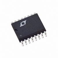
LTC1064-2CSW Linear Technology, LTC1064-2CSW Datasheet

LTC1064-2CSW
Specifications of LTC1064-2CSW
Available stocks
Related parts for LTC1064-2CSW
LTC1064-2CSW Summary of contents
Page 1
... In fact the LTC1064-2 overall performance competes with equivalent multiple op amp RC active realizations. The LTC1064-2 is available in a 14-pin DIP or 16-pin surface mounted SW package. The LTC1064-2 is fabricated using LTC’s enhanced analog CMOS Si-gate process. The LTC1064-2 is pin compatible with the LTC1064-1. ...
Page 2
... IN = ±2.37V = ±5V = ±7.5V = ±5V, Input = 1V at 1kHz RMS = ±7.5V, Input = 3V at 1kHz RMS = ±5V, Input = GND 1Hz – 1.99MHz = ±7.5V, Input = GND 1Hz – 1.99MHz ORDER PART NUMBER TOP VIEW 16 OUT C LTC1064-2CSW 15 NC – CLK 11 50/100 OUT SW PACKAGE = 150°C, θ ...
Page 3
... A f –45 CLK 100:1 –90 f –3dB –135 –180 –225 –270 –315 –360 –405 –450 (kHz) IN LTC1064-2 = 2MHz 10k, TTL clock input level unless CLK MIN TYP ±30 ± 3/1 200 ±2.37 Group Delay vs Frequency 220 V = ±7.5V S 200 T = 25° 1MHz f = 1MHz ...
Page 4
... LTC1064 TYPICAL PERFOR A CE CHARACTERISTICS Phase vs f Frequency –3dB 2MHz CLK 40kHz –3dB – 500kHz CLK – 10kHz –3dB – 1MHz –120 CLK f = 20kHz –3dB –150 –180 –210 V = ±7.5V –240 S 50:1 –270 100 1k 10k FREQUENCY (Hz) 1064 G04 Harmonic Distortion vs Frequency 0.1 ...
Page 5
... Table 4. Gain 25°C, LTC1064-2 Typical Response 100kHz, Ratio = Pin CLK GAIN (dB) FREQUENCY (kHz) –0.298 –3.380 –27.500 –47.200 –63.300 –75.190 –86.100 –95.310 –104.240 –109.650 –121.930 –123.920 – ...
Page 6
... Table 6. Gain 25°C, LTC1064-2 Typical Response 7MHz, Ratio = Pin CLK GAIN (dB) FREQUENCY (kHz) –0.308 –3.350 –27.400 –47.100 –62.300 –74.890 –85.430 –95.070 –103.150 –108.700 –107.520 –108.030 – ...
Page 7
... For ±7V sup- plies and above, the maximum clock frequency is 7MHz. Do not allow the clock levels to exceed the power supplies. For single supply operation ≥6V use level shifting at Pin 11 2 with T L levels (Figure 4). + and LTC1064-2 + and 100:1 when – 10642fa 7 ...
Page 8
... RECOMMENDED OP AMPS: LT1022, LT318, LT1056 Figure 1. Buffering the Filter Output. The Buffer Op Amp Should Not Share the LTC1064-2 Power Lines 15V Figure 3. Single Supply Operation. If Fast Power Up or Down Transients are Expected, Use a 1N5817 Schottky Diode Between Pin 4 and Pin 5. For V with a 7 ...
Page 9
... Figure 4. Level Shifting the Input T for Single Supply Operation ≥6V. 14 OUT – V LTC1064-2 12 – V 0.1µ CLK 10 + – 50/100 V /GND/V 10k 10k 9 V OUT 220pF LTC1064 2. LEVEL 5k 1µ Clock 20k V OUT 100pF 15V – 50Ω LT1056 + 0.027µF 1064-2 F05 –15V 10642fa 9 ...
Page 10
... LTC1064-2 PACKAGE DESCRIPTIO .300 BSC (7.62 BSC) .008 – .018 (0.203 – 0.457) NOTE: LEAD DIMENSIONS APPLY TO SOLDER DIP/PLATE OR TIN PLATE LEADS Package 14-Lead CERDIP (Narrow 0.300, Hermetic) (LTC DWG # 05-08-1110) .785 (19.939) .005 MAX (0.127) MIN .025 (0.635) RAD TYP ...
Page 11
... MIN .005 .120 (0.125) .100 (3.048) MIN (2.54) MIN BSC LTC1064-2 .770* (19.558) MAX .045 – .065 .065 (1.651) TYP .018 ± .003 (0.457 ± 0.076) N14 1002 ...
Page 12
... LTC1064-2 PACKAGE DESCRIPTIO .030 ±.005 TYP N .420 MIN RECOMMENDED SOLDER PAD LAYOUT .291 – .299 (7.391 – 7.595) NOTE 4 .010 – .029 × 45° (0.254 – 0.737) .005 (0.127) RAD MIN .009 – .013 NOTE 3 (0.229 – 0.330) .016 – .050 (0.406 – ...


