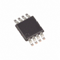
MAX7421CUA+T Maxim Integrated Products, MAX7421CUA+T Datasheet - Page 9

MAX7421CUA+T
Manufacturer Part Number
MAX7421CUA+T
Description
IC FILTER LOWPASS 5TH 8UMAX
Manufacturer
Maxim Integrated Products
Datasheet
1.MAX7421EUA.pdf
(14 pages)
Specifications of MAX7421CUA+T
Filter Type
Elliptic, Lowpass Switched Capacitor
Frequency - Cutoff Or Center
45kHz
Number Of Filters
1
Max-order
5th
Voltage - Supply
4.5 V ~ 5.5 V
Mounting Type
Surface Mount
Package / Case
8-MSOP, Micro8™, 8-uMAX, 8-uSOP,
For Use With
MAXFILTERBRD+ - BOARD EVAL MAX7408/7415/418-7425
Lead Free Status / RoHS Status
Lead free / RoHS Compliant
The MAX7418/MAX7421/MAX7422/MAX7425 elliptic
lowpass filters provide sharp rolloff with good stopband
rejection. The MAX7419/MAX7423 Bessel filters provide
low overshoot and fast settling responses, and the
MAX7420/MAX7424 Butterworth filters provide a maxi-
mally flat passband response. All parts operate with a
100:1 clock-to-corner frequency ratio.
Most switch capacitor filters (SCFs) are designed with
biquadratic sections. Each section implements two
pole-zero pairs, and the sections can be cascaded to
_______________Detailed Description
(V
T
A
DD
PIN
= +25°C; unless otherwise noted.)
1
2
3
4
5
6
7
8
= +5V for MAX7418–MAX7421, V
NAME
SHDN
COM
GND
OUT
V
CLK
3.0
2.5
2.0
1.5
1.0
0.5
OS
IN
0
DD
-40
_______________________________________________________________________________________
-15
Common Input Pin. Biased internally at midsupply. Bypass COM externally to GND with a 0.1µF capacitor.
To override internal biasing, drive COM with an external supply.
Filter Input
Ground
Positive Supply Input: +5V for MAX7418–MAX7421, +3V for MAX7422–MAX7425. Bypass V
0.1µF capacitor.
Filter Output
Offset Adjust Input. To adjust output offset, connect OS to an external supply through a resistive voltage-
divider (Figure 4). Connect OS to COM if no offset adjustment is needed. The Offset and Common-Mode
Input Adjustment section.
Shutdown Input. Drive low to enable shutdown mode; drive high or connect to V
Clock Input. Connect an external capacitor (C
connect CLK to an external clock: f
DC OFFSET VOLTAGE
vs. TEMPERATURE
TEMPERATURE (°C)
10
V
35
DD
= 3V
V
DD
DD
= 5V
60
= +3V for MAX7422–MAX7425; f
Typical Operating Characteristics (continued)
85
Switched-Capacitor Filters
C
= f
CLK
/100.
produce higher order filters. The advantage to this
approach is ease of design. However, this type of
design is highly sensitive to component variations if any
section’s Q is high. The MAX7418–MAX7425 use an
alternative approach, which is to emulate a passive net-
work using switched-capacitor integrators with sum-
ming and scaling. The passive network may be
synthesized using CAD programs, or may be found in
many filter books. Figure 1 shows a basic 5th-order lad-
der filter structure.
OSC
FUNCTION
) from CLK to ground. To override the internal oscillator,
5th-Order, Lowpass,
CLK
= 2.2MHz; SHDN = V
2.5
2.0
1.5
1.0
0.5
0
2.5
3.0
vs. SUPPLY VOLTAGE
DC OFFSET VOLTAGE
SUPPLY VOLTAGE (V)
3.5
DD
DD
4.0
Pin Description
for normal operation.
; V
COM
4.5
DD
= V
5.0
to GND with a
OS
5.5
= V
DD
/ 2;
9


