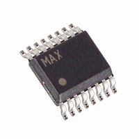
MAX7490CEE+ Maxim Integrated Products, MAX7490CEE+ Datasheet

MAX7490CEE+
Specifications of MAX7490CEE+
Related parts for MAX7490CEE+
MAX7490CEE+ Summary of contents
Page 1
... Internal Sampling-to-Center Frequency Ratio of 200:1 o Center Frequency up to 40kHz o Easily Cascaded for Multipole Filters o Low-Power Shutdown: < 1µA Supply Current Ordering Information PIN- PART TEMP RANGE PACKAGE MAX7490CEE+ 0°C to +70°C 16 QSOP MAX7490EEE+ -40°C to +85°C 16 QSOP MAX7491CEE+ 0°C to +70°C 16 QSOP MAX7491EEE+ -40° ...
Page 2
Dual Universal Switched-Capacitor Filters ABSOLUTE MAXIMUM RATINGS V to GND ..............................................................-0.3V to +6V DD EXTCLK, SHDN to GND ...........................................-0.3V to +6V INV_, LP_, BP_, N_/HP_, S_, COM, CLK to GND............................................-0. Maximum Current into Any Pin ...........................................50mA Continuous Power ...
Page 3
Dual Universal Switched-Capacitor Filters ELECTRICAL CHARACTERISTICS—MAX7490 (continued +5V 625kHz; 10kΩ || 50pF load to V EXTCLK DD CLK GND; 50% duty-cycle clock input; COM = V (Note 1) PARAMETER SYMBOL Clock Input Low Clock ...
Page 4
Dual Universal Switched-Capacitor Filters ELECTRICAL CHARACTERISTICS—MAX7491 ( +3V 625kHz; 10kΩ || 50pF load to V EXTCLK DD CLK GND; 50% duty-cycle clock input; COM = V (Note 1) PARAMETER SYMBOL FILTER Center Frequency Range Clock-to-Center ...
Page 5
Dual Universal Switched-Capacitor Filters ELECTRICAL CHARACTERISTICS—MAX7491 (continued +3V 625kHz; 10kΩ || 50pF load EXTCLK CLK GND; 50% duty-cycle clock input; COM = V (Note 1) PARAMETER SYMBOL POWER REQUIREMENTS Supply Voltage ...
Page 6
Dual Universal Switched-Capacitor Filters (V = +5V for MAX7490 +3V for MAX7491 10kΩ +25°C, unless otherwise noted.) A CLOCK-TO-CENTER FREQUENCY DEVIATION vs ...
Page 7
Dual Universal Switched-Capacitor Filters (V = +5V for MAX7490 +3V for MAX7491 10kΩ +25°C, unless otherwise noted.) A MAX7490 THD + NOISE vs. FREQUENCY - MODE ...
Page 8
Dual Universal Switched-Capacitor Filters NAME PIN FILTER A LP_ 1 BP_ 2 N_/HP_ 3 INV_ SHDN 6 GND CLK 9 EXTCLK 10 COM 11 _______________Detailed Description The MAX7490/MAX7491 are universal switched-capaci- tor filters ...
Page 9
Dual Universal Switched-Capacitor Filters (6) SHDN V ( GND (7) CLK (9) EXTCLK (10) Figure 1. Block Diagram 2nd-Order Filter Stage The MAX7490/MAX7491 are dual biquad filters. The biquad topology allows the use of standard filter tables ...
Page 10
Dual Universal Switched-Capacitor Filters Table 1. Filter Operating Modes MODE • • 1 • • 1B • • • • • 3 • • • LP-N = lowpass notch, HP-N = highpass notch. ...
Page 11
Dual Universal Switched-Capacitor Filters Σ COM Figure 2. Mode 1, 2nd-Order Filter Providing Notch, Bandpass, and Lowpass Outputs Figure 2 shows the MAX7490/MAX7491s’ configuration of Mode 1. This mode ...
Page 12
Dual Universal Switched-Capacitor Filters Mode 2 Design Equations CLK = + 100 CLK = f n 100 ⎛ ⎞ ...
Page 13
Dual Universal Switched-Capacitor Filters Figure 6 shows the configuration of Mode 3. This mode is a sampled time (Z transform) equivalent of the classi- cal 2nd-order state variable filter. In this versatile mode, the ratio of resistors R2 and R4 ...
Page 14
Dual Universal Switched-Capacitor Filters Table 3. Suggested External Op Amps PART GBW (MHz) MAX4281 2 MAX4322 5 MAX4130 10 MAX4490 10 Mode 3A Design Equations CLK = f O 100 CLK H = ...
Page 15
Dual Universal Switched-Capacitor Filters Table 4. Output DC Offsets for a 2nd-Order Section MODE V OSN/ (R2 / R3) + ( OS1 1 ( (R2 / R3) + ...
Page 16
Dual Universal Switched-Capacitor Filters Table 5. Cascading Identical Bandpass Filter Sections TOTAL SECTIONS TOTAL BW 1 1.000 B 2 0.644 B 3 0.510 B 4 0.435 B 5 0.386 B The wideband noise of the filter is the total RMS ...
Page 17
Dual Universal Switched-Capacitor Filters 4TH-ORDER 10kHz BANDPASS FILTER LPA R3A 200k BPA R2A 10k NA/HPA R1 200k V INVA IN SA SHDN GND 0.1μF Package Information For the latest package outline information and land patterns, ...
Page 18
... Maxim cannot assume responsibility for use of any circuitry other than circuitry entirely embodied in a Maxim product. No circuit patent licenses are implied. Maxim reserves the right to change the circuitry and specifications without notice at any time. 18 ____________________Maxim Integrated Products, 120 San Gabriel Drive, Sunnyvale, CA 94086 408-737-7600 © 2009 Maxim Integrated Products DESCRIPTION Maxim is a registered trademark of Maxim Integrated Products, Inc ...


