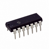
MCP25055-I/P Microchip Technology, MCP25055-I/P Datasheet - Page 28

MCP25055-I/P
Manufacturer Part Number
MCP25055-I/P
Description
IC I/O EXPANDER CAN 8B 14DIP
Manufacturer
Microchip Technology
Specifications of MCP25055-I/P
Mounting Type
Through Hole
Interface
1-Wire, CAN
Number Of I /o
8
Interrupt Output
No
Frequency - Clock
4MHz
Voltage - Supply
2.7 V ~ 5.5 V
Operating Temperature
-40°C ~ 85°C
Package / Case
14-DIP (0.300", 7.62mm)
Includes
ADC, Memory, PWM
Bus Frequency
4MHz
No. Of I/o's
8
Supply Voltage Range
2.7V To 5.5V
Digital Ic Case Style
DIP
No. Of Pins
14
Operating Temperature Range
-40°C To +85°C
Data Rate Max
1Mbps
Leaded Process Compatible
Yes
Rohs Compliant
Yes
Lead Free Status / RoHS Status
Lead free / RoHS Compliant
For Use With
DV250501 - KIT DEV CAN MCP250XX
Lead Free Status / RoHS Status
Lead free / RoHS Compliant, Lead free / RoHS Compliant
Other names
MCP25055I/P
Available stocks
Company
Part Number
Manufacturer
Quantity
Price
Company:
Part Number:
MCP25055-I/P
Manufacturer:
MICROCHIP
Quantity:
12 000
MCP2502X/5X
If
(OPTREG2.TXONE = 1) and one of the above
conditions occur, the MCP2502X/5X sends TXID1
identifier with output message Read CAN Error States
data field (three data bytes).
4.5.4
The MCP2502X/5X has the capability of sending
scheduled transmissions (On Bus message), if
enabled.
The scheduled transmission control register (STCON)
enables and configures the occurrence of the
scheduled message. Setting the STEN bit in the
STCON register enables the scheduled message. The
STBF1:STBF0 and STM3:STM0 bits allow a scheduled
transmission to be initiated from a minimum of 256 µs
to a maximum of 16.8 seconds (using a 16 MHz
and the following equation:
REGISTER 4-1:
DS21664D-page 28
the
Error
bit 7
bit 6
bit 5-4
bit 3-0
SCHEDULED TRANSMISSIONS
Condition
STCON - SCHEDULED TRANSMISSION CONTROL REGISTER
STEN: Scheduled Transmission Enable bits
1 = Enabled
0 = Disabled
STMS: Scheduled Transmission Message Select
1 = Sends Transmit ID 0 (TXID0) with the “Read A/D Regs” data (DLC = 8)
0 = Sends Transmit ID 0 (TXID0) with no data (DLC = 0)
STBF1:STBF0: Base Transmission Frequency bits
00 = 4096T
01 = 16
10 = 256
10 = 4096
(e.g., STBF1:STBF0 => 00 => 256 µs for a 16 MHz F
STM3:STM0: Scheduled Transmission Multiplier bits
0000 = 1
0001 = 2
-
-
1110 = 15
1111 = 16
Legend:
R = Readable bit
- n = Value at POR
bit 7
R/W-0
STEN
message
•
(4096T
•
(4096T
•
(4096T
OSC
R/W-0
STMS
OSC
OSC
OSC
is
)
)
)
enabled
STBF1
F
R/W-1
OSC
W = Writable bit
‘1’ = Bit is set
)
STBF0
R/W-1
Message Type - The message sent for scheduled
transmissions consists of either TXID0 with zero data
bytes or TXID0 with eight data bytes containing the
Read A/D Regs message, depending on STMS bit in
the STCON register.
Note:
U = Unimplemented bit, read as ‘0’
‘0’ = Bit is cleared
Scheduled Transmission
R/W-1
STM3
The
intervals may vary slightly due to the
internal event que of the control module.
OSC
= STBF1:STBF0(STM3:STM0)
)
actual
R/W-1
STM2
© 2007 Microchip Technology Inc.
scheduled
x = Bit is unknown
R/W-1
STM1
transmission
R/W-1
STM0
bit 0


