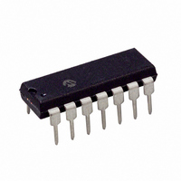
MCP25055-I/P Microchip Technology, MCP25055-I/P Datasheet - Page 35

MCP25055-I/P
Manufacturer Part Number
MCP25055-I/P
Description
IC I/O EXPANDER CAN 8B 14DIP
Manufacturer
Microchip Technology
Specifications of MCP25055-I/P
Mounting Type
Through Hole
Interface
1-Wire, CAN
Number Of I /o
8
Interrupt Output
No
Frequency - Clock
4MHz
Voltage - Supply
2.7 V ~ 5.5 V
Operating Temperature
-40°C ~ 85°C
Package / Case
14-DIP (0.300", 7.62mm)
Includes
ADC, Memory, PWM
Bus Frequency
4MHz
No. Of I/o's
8
Supply Voltage Range
2.7V To 5.5V
Digital Ic Case Style
DIP
No. Of Pins
14
Operating Temperature Range
-40°C To +85°C
Data Rate Max
1Mbps
Leaded Process Compatible
Yes
Rohs Compliant
Yes
Lead Free Status / RoHS Status
Lead free / RoHS Compliant
For Use With
DV250501 - KIT DEV CAN MCP250XX
Lead Free Status / RoHS Status
Lead free / RoHS Compliant, Lead free / RoHS Compliant
Other names
MCP25055I/P
Available stocks
Company
Part Number
Manufacturer
Quantity
Price
Company:
Part Number:
MCP25055-I/P
Manufacturer:
MICROCHIP
Quantity:
12 000
REGISTER 5-7:
TABLE 5-2:
© 2007 Microchip Technology Inc.
Bank 0
Addr
34h
00h
01h
04h
Legend: x = unknown, U = unchanged, - = unimplemented read as ‘0’. Shaded cells are not used by module.
OPTREG1
IOINTEN
IOINTPO
GPDDR
Name
bit 7
bit 6
bit 5
bit 4
bit 3
bit 2
bit 1
bit 0
SUMMARY OF REGISTERS ASSOCIATED WITH GPIO MODULE
GP7TXC
GP7POL
GPPU
bit7
—
CAEN: Command Acknowledge Enable bit
1 = Enables the command acknowledge message (TXID1)
0 = Enables the receive overflow message (TXID1)
ERREN: Error Recovery Enable bit
1 = MCP2502X/5X will recover into Listen-only mode from bus off
0 = MCP2502X/5X will recover into Normal mode from bus-off
TXONEN: Transmit on Error Condition bit(REC or TEC)
1 = Enable, will send message if error counter(s) go high enough
0 = Disable, will NOT send message regardless of error counter values
SLPEN: Low power SLEEP mode enable/disable
1 = Device will enter Sleep if bus is idle for at least 1408 bit times
0 = SLEEP mode is disabled
MTYPE: Determines if information request messages use RTR or not
1 = RTR is NOT used for IRM (Data Frame)
0 = RTR is used for IRM (Remote Frame)
PDEFEN: Enables PWM outputs to return to POR default values when CAN bus communication
is lost
1 = Enables PWM output default values
0 = Disables PWM output default values
PUSLP: Allows device to enter SLEEP while in Listen-only mode during power-up sequence
1 = Enables SLEEP when in Listen-only mode during power-up sequence
0 = Disables SLEEP when in Listen-only mode during power-up sequence
PUNRM: Enters Normal mode after completing self-configuration during power-up sequence
1 = Enters “Normal” mode after completing self-configuration during power-up sequence
0 = Enables “Listen-only” mode after completing self-configuration during power-up sequence
Legend:
R = Readable bit
- n = Value at POR
OPTREG2 REGISTER
bit 7
R/W-0
CAEN
and waits for an error-free message before switching to Normal mode
GP6TXC
GP6POL
CLKEN
DDR6
bit6
ERREN
R/W-0
GP5TXC
GP5POL
CLKPS1
DDR5
bit5
TXONEN
GP4TXC
GP4POL
CLKPS0
R/W-0
DDR4
bit4
W = Writable bit
‘1’ = Bit is set
GP3TXC
GP3POL
DDR3
SLPEN
bit3
R/W-0
—
GP2TXC
GP2POL
CMREQ
DDR2
bit2
MTYPE
R/W-0
U = Unimplemented bit, read as ‘0’
‘0’ = Bit is cleared
GP1TXC
GP1POL
DDR1
AQT1
bit1
MCP2502X/5X
PDEFEN
R/W-0
GP0TXC
GP0POL
DDR0
AQT0
bit0
x = Bit is unknown
-111 1111 -111 1111
0000 0000 0000 0000
0000 0000 0000 0000
0000 ---- 0000 ----
PUSLP
R/W-0
Value on
POR
DS21664D-page 35
PUNRM
Value on
R/W-0
RST
bit 0


