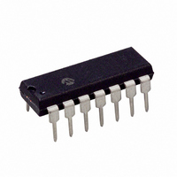
MCP25055-I/P Microchip Technology, MCP25055-I/P Datasheet - Page 37

MCP25055-I/P
Manufacturer Part Number
MCP25055-I/P
Description
IC I/O EXPANDER CAN 8B 14DIP
Manufacturer
Microchip Technology
Specifications of MCP25055-I/P
Mounting Type
Through Hole
Interface
1-Wire, CAN
Number Of I /o
8
Interrupt Output
No
Frequency - Clock
4MHz
Voltage - Supply
2.7 V ~ 5.5 V
Operating Temperature
-40°C ~ 85°C
Package / Case
14-DIP (0.300", 7.62mm)
Includes
ADC, Memory, PWM
Bus Frequency
4MHz
No. Of I/o's
8
Supply Voltage Range
2.7V To 5.5V
Digital Ic Case Style
DIP
No. Of Pins
14
Operating Temperature Range
-40°C To +85°C
Data Rate Max
1Mbps
Leaded Process Compatible
Yes
Rohs Compliant
Yes
Lead Free Status / RoHS Status
Lead free / RoHS Compliant
For Use With
DV250501 - KIT DEV CAN MCP250XX
Lead Free Status / RoHS Status
Lead free / RoHS Compliant, Lead free / RoHS Compliant
Other names
MCP25055I/P
Available stocks
Company
Part Number
Manufacturer
Quantity
Price
Company:
Part Number:
MCP25055-I/P
Manufacturer:
MICROCHIP
Quantity:
12 000
6.0
6.1
There are two Pulse Width Modulation (PWM) modules
(PWM1 and PWM2) that generate up to a 10-bit
resolution output signal on GP2 and GP3, respectively.
Each of these outputs can be separately enabled, with
each having its own associated timer, duty cycle and
period registers for controlling the PWM output shape.
Each PWM module contains a set of master/slave duty
cycle registers, providing up to a 10-bit resolution PWM
output. Figure 6-1 shows a simplified block diagram of
the PWM module. A PWM output has a time base
(period) and a time that the output stays high (duty
cycle), as shown in Figure 6-2. The frequency of the
PWM is the inverse of the period (1/period).
At power-on, the PWM outputs are not enabled until
after the self-configuration sequence has been
completed (i.e., all SRAM registers have been loaded
with their default values) to prevent invalid signals from
occurring on the PWM outputs.
FIGURE 6-1:
The PWM outputs can be forced to their default POR
conditions if CAN bus communication is lost and is
enabled via OPTREG2.PDEFEN. The system designer
must implement a hand-shaking protocol, such that the
MCP2505X will receive a valid message into one of the
receive buffers before four successive scheduled
transmissions occur. If a valid message is not received,
the PWM outputs GP2 and GP3 will automatically
© 2007 Microchip Technology Inc.
PWMnDCH
PWMnDBH
Comparator
Note 1:
TMRn
Comparator
Prn
Duty cycle
registers
PWM MODULE
Description
8-bit timer is concatenated with 2-bit internal
Q clock or 2 bits of the prescaler to create
10-bit time base
Note
1
TnCON
(2 LSB)
SIMPLIFIED BLOCK
DIAGRAM
R
S
Q
DDR<Y>
(PWMn)
GP<Y>
reconfigure to their default conditions. This includes the
PWM module itself being disabled and the GPIO being
forced low, high or tri-state.
FIGURE 6-2:
6.2
There are two 8-bit timers supporting the two PWM
outputs. Both timers have a prescaler only. The timers
are readable and writable and are cleared on any
device reset or when the timer is turned off.
The input clock (F
1:4 or 1:16, selected by control bits TnCKPS[1:0] in
register TnCON<5:4> (where n corresponds to the
appropriate timer).
Each timer module has an 8-bit period register, PRn.
PRn is a readable and writable register. The timer
module increments from 00h until it matches PRn and
then resets to 00h on the next increment cycle. The
PRn register is set when the device is reset.
Each timer can be shut off by clearing control bit
TMRnON (TnCON<7>).
6.2.1
The prescaler counters are cleared when a write to the
TnCON or TMRn register or any device reset (RST
reset or Power-on reset) occurs.
6.3
Each PWM module contains a set of master/slave duty
cycle registers, providing up to a 10-bit resolution PWM
output. Figure 6-2 shows a simplified block diagram of
the PWM module.
6.3.1
The PWM period is specified by writing to the PRn
register. The PWM period can be calculated using the
following formula:
When TMRn is equal to PRn, the following two events
occur on the next cycle:
• TMRn is cleared
• The PWM duty cycle is latched from PWMnDCH
PWM period
into PWMnDBH
TMRn = PRn
Duty Cycle
PWM Timer Modules
PWM Modules
PWM frequency
TIMER MODULE PRESCALER
PWM PERIOD
=
Period
[
(
PR n
MCP2502X/5X
TMRn=Duty Cycle
OSC
)
+
/4) has a prescale option of 1:1,
PWM OUTPUT
TMRn = PRn
1
]*4T OSC * TMRn prescale value
=
1
⁄
(
PWM period
(
DS21664D-page 37
)
)


