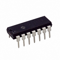
MCP25055-I/P Microchip Technology, MCP25055-I/P Datasheet - Page 8

MCP25055-I/P
Manufacturer Part Number
MCP25055-I/P
Description
IC I/O EXPANDER CAN 8B 14DIP
Manufacturer
Microchip Technology
Specifications of MCP25055-I/P
Mounting Type
Through Hole
Interface
1-Wire, CAN
Number Of I /o
8
Interrupt Output
No
Frequency - Clock
4MHz
Voltage - Supply
2.7 V ~ 5.5 V
Operating Temperature
-40°C ~ 85°C
Package / Case
14-DIP (0.300", 7.62mm)
Includes
ADC, Memory, PWM
Bus Frequency
4MHz
No. Of I/o's
8
Supply Voltage Range
2.7V To 5.5V
Digital Ic Case Style
DIP
No. Of Pins
14
Operating Temperature Range
-40°C To +85°C
Data Rate Max
1Mbps
Leaded Process Compatible
Yes
Rohs Compliant
Yes
Lead Free Status / RoHS Status
Lead free / RoHS Compliant
For Use With
DV250501 - KIT DEV CAN MCP250XX
Lead Free Status / RoHS Status
Lead free / RoHS Compliant, Lead free / RoHS Compliant
Other names
MCP25055I/P
Available stocks
Company
Part Number
Manufacturer
Quantity
Price
Company:
Part Number:
MCP25055-I/P
Manufacturer:
MICROCHIP
Quantity:
12 000
MCP2502X/5X
The base T
Adding the BRP into the equation yields:
By definition, the nominal bit time is programmable
from a minimum of 8 T
nominal bit time is 1 µs, which corresponds to 1 Mb/s.
2.4.2
Time segments make up the nominal bit time. The
nominal bit time can be thought of as being divided into
separate non-overlapping time segments. These
segments are shown in Figure 2-3.
• Synchronization Segment (SyncSeg)
• Propagation Segment (PropSeg)
• Phase Buffer Segment 1 (PS1)
• Phase Buffer Segment 2 (PS2)
Rules for Programming the Segments
There are a few rules to follow when programming the
time segments:
• PropSeg + PS1 ≥ PS2
• PS2 > Sync Jump Width
• PS2 ≥ Information Processing Time
2.4.2.1
This part of the bit time is used to synchronize the
various CAN nodes on the bus. The edge of the input
signal is expected to occur during the SyncSeg. The
duration is fixed at 1 T
2.4.2.2
This part of the bit time is used to compensate for
physical delay times within the network. These delay
times consist of the signal propagation time on the bus
line and the internal delay time of the nodes. The delay
is calculated as being the round-trip time from
transmitter to receiver (twice the signal's propagation
time on the bus line), the input comparator delay and
the output driver delay. The length of the Propagation
Segment can be programmed from 1 T
setting the PRSEG2:PRSEG0 bits of the CNF2
register.
DS21664D-page 8
Nominal Bit Time
where BRP = binary value represented by
Q
TIME SEGMENTS
Synchronization Segment
Propagation Segment
is defined as twice the oscillator period.
T
Q
CNF1.BRP<5:0>
=
=
+
2*T
T
Phase_Seg1
Q
Q
Q
.
OSC
* Sync_Seg
to 25 T
(
* BRP
(
Q
. Also, the minimum
+
+
Phase_Seg2
1
+
)
PropSeg
Q
to 8 T
Q
)
by
2.4.2.3
The Phase Buffer Segments are used to optimally
locate the sampling point of the received bit within the
nominal bit time. The sampling point occurs between
PS1 and PS2. These segments can be automatically
lengthened or shortened by the resynchronization
process. Thus, the variation of the values of the phase
buffer segments represent the DPLL functionality.
Phase Segment 1 (PS1): The end of PS1 determines
the sampling point within a bit time. PS1 is programma-
ble from 1 T
Phase Segment 2 (PS2): PS2 provides delay before
the next transmitted data transition and is also pro-
grammable from 1 T
to IPT requirements, the actual minimum length of
phase segment 2 is 2 T
equal to the greater of PS1 or the information process-
ing time (IPT).
2.4.3
The sample point is the point of time at which the bus
level is read and the value of the received bit is
determined. The sampling point occurs at the end of
PS1. If desired, it is possible to specify multiple
sampling of the bus line at the sample point. The value
of the received bit is determined to be the value of the
majority decision of three values. The three samples
are taken at the sample point, and twice before, with a
time of T
2.4.4
The Information Processing Time (IPT) is the time
segment (starting at the sample point) that is reserved
for calculation of the subsequent bit level. The CAN
specification defines this time to be less than or equal
to 2 T
2 T
2.4.5
To compensate for phase shifts and oscillator
tolerances between the nodes in the system, each
CAN controller must be able to synchronize to the
relevant signal edge of the incoming signal. When a
recessive-to-dominant edge in the transmitted data is
detected, the logic will compare the location of the edge
to the expected time (SyncSeg). The circuit will then
adjust the values of PS1 and PS2, as necessary, using
the programmed Synchronization Jump Width (SJW).
This adjustment is made for resynchronization during a
message and not hard synchronization, which occurs
only at the message Start-of-Frame (SOF).
Q
. Thus, PS2 must be at least 2 T
Q
. The MCP2502X/5X defines this time to be
Q
/2 between each sample.
SAMPLE POINT
INFORMATION PROCESSING TIME
SYNCHRONIZATION JUMP WIDTH
Q
Phase Buffer Segments
- 8 T
Q
Q
in duration.
- 8 T
Q
© 2007 Microchip Technology Inc.
. It may also be defined to be
Q
in duration. However, due
Q
long.


