PCA9698DGG,512 NXP Semiconductors, PCA9698DGG,512 Datasheet
PCA9698DGG,512
Specifications of PCA9698DGG,512
935278614512
PCA9698DGG
Available stocks


Related parts for PCA9698DGG,512


PCA9698DGG,512 Summary of contents
Page 1
PCA9698 40-bit Fm+ I Rev. 3 — 3 August 2010 1. General description The PCA9698 provides 40-bit parallel input/output (I/O) port expansion for I applications organized in 5 banks of 8 I/Os supply voltage, the outputs are ...
Page 2
... NXP Semiconductors 2 5.5 V operation with 5.5 V tolerant I/Os 40 configurable I/O pins that default to inputs at power-up Outputs: Programmable totem-pole (10 mA source sink) or open-drain (25 mA sink) with controlled edge rate output structure. Default to totem-pole on power-up. Active LOW Output Enable (OE) input pin 3-states all outputs. Polarity can be ...
Page 3
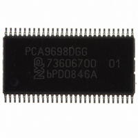
... NXP Semiconductors 4. Ordering information Table 1. Ordering information − ° ° +85 C amb Type number Topside mark PCA9698DGG PCA9698DGG PCA9698BS PCA9698BS 5. Block diagram AD0 AD1 AD2 SCL SDA RESET Fig 1. PCA9698 Product data sheet 2 40-bit Fm+ I C-bus advanced I/O port with RESET, OE and INT ...
Page 4
... NXP Semiconductors data from shift register write configuration pulse data from shift register OCH write pulse CK read pulse data from shift register write polarity pulse On power-up or RESET, all registers return to default values. Fig 2. Simplified schematic of the I/Os (IO0_0 to IO4_7) PCA9698 Product data sheet ...
Page 5
... NXP Semiconductors 6. Pinning information 6.1 Pinning Fig 3. PCA9698 Product data sheet 2 40-bit Fm+ I C-bus advanced I/O port with RESET, OE and INT SDA 1 SCL 2 3 IO0_0 4 IO0_1 IO0_2 IO0_3 7 8 IO0_4 9 IO0_5 IO0_6 IO0_7 12 13 IO1_0 14 IO1_1 PCA9698DGG IO1_2 15 IO1_3 16 IO1_4 17 18 ...
Page 6
... NXP Semiconductors Fig 4. 6.2 Pin description Table 2. Symbol SDA SCL IO0_0 to IO0_7 IO1_0 to IO1_7 IO2_0 to IO2_7 IO3_0 to IO3_7 IO4_0 to IO4_7 AD0 AD1 PCA9698 Product data sheet 2 40-bit Fm+ I C-bus advanced I/O port with RESET, OE and INT terminal 1 index area IO0_4 1 IO0_5 ...
Page 7
... NXP Semiconductors Table 2. Symbol AD2 OE INT/SMBALERT RESET [1] HVQFN56 package die supply ground is connected to both V must be connected to supply ground for proper device operation. For enhanced thermal, electrical, and board level performance, the exposed pad needs to be soldered to the board using a corresponding thermal pad on the board and for proper heat conduction through the board, thermal vias need to be incorporated in the printed-circuit board in the thermal pad region ...
Page 8
... NXP Semiconductors 7.2 Alert response, GPIO All Call and Device ID addresses Three other different addresses can be sent to the PCA9698. • Alert Response address: allows to perform an ‘SMBus Alert’ operation as defined in the SMBus specification. This address is always used to perform a Read operation. See • ...
Page 9
... NXP Semiconductors 7.3.1 5-bank register category • IP – Input registers • OP – Output registers • PI – Polarity Inversion registers • IOC – I/O Configuration registers • MSK – Mask interrupt registers If the Auto-Increment flag is set (AI = 1), the 3 least significant bits are automatically incremented after a read or write ...
Page 10
... NXP Semiconductors Table 3. Register summary …continued Reg # Output Port registers 08h 09h 0Ah 0Bh 0Ch 0Dh 0Eh 0Fh Polarity Inversion registers 10h 11h 12h 13h 14h 15h 16h 17h I/O Configuration registers 18h 19h 1Ah 1Bh 1Ch 1Dh 1Eh 1Fh Mask Interrupt registers ...
Page 11
... NXP Semiconductors 7.4.1 IP0 to IP4 - Input Port registers These registers are read-only. They reflect the incoming logic levels of the port pins regardless of whether the pin is defined as an input or an output by the I/O Configuration register. If the corresponding Px[y] bit in the PI registers is set the inverted incoming logic levels if the corresponding Px[y] bit in the PI register is set to 1 ...
Page 12
... NXP Semiconductors 7.4.3 PI0 to PI4 - Polarity Inversion registers These registers allow inversion of the polarity of the corresponding Input Port register. Px[ The corresponding Input Port register data polarity is retained. Px[ The corresponding Input Port register data polarity is inverted. Where ‘x’ refers to the bank number (0 to 4); ‘y’ refers to the bit number (0 to 7). ...
Page 13
... NXP Semiconductors 7.4.5 MSK0 to MSK4 - Mask interrupt registers These registers mask the interrupt due to a change in the I/O pins configured as inputs. ‘x’ refers to the bank number (0 to 4); ‘y’ refers to the bit number (0 to 7). Mx[ level change at the I/O will generate an interrupt if IOx_y defined as input (Cx[y] in IOC register = 1) ...
Page 14
... NXP Semiconductors 7.4.7 ALLBNK - All Bank control register Table 10. Bit Symbol Default This register allows all the I/Os configured as outputs to be programmed with the same logic value. This programming is applied to all the banks or a selection of banks. When this register is programmed, values in the Output Port registers are not changed and do not reflect the states of I/Os configured as outputs anymore. • ...
Page 15
... NXP Semiconductors • If ALLBNK = 1XX0 1100: All I/Os configured as outputs in Bank 2 and 3 will be programmed with 1s, overwriting values programmed in the Output Port registers 2 and 3, while I/Os configured as outputs in Bank 0, 1, and 4 are programmed with values in Output Port registers 0, 1, and 4. 7.4.8 MODE - PCA9698 mode selection register Table 11 ...
Page 16
... NXP Semiconductors 7.5 Device ID - PCA9698 ID field The Device ID field byte read-only (24 bits) word giving the following information: • 12 bits with the manufacturer name, unique per manufacturer (e.g., NXP) • 9 bits with the part identification, assigned by manufacturer (e.g., PCA9698) • 3 bits with the die revision, assigned by manufacturer (e.g., RevX) The Device ID is read-only, hard-wired in the device and can be accessed as follows: 1 ...
Page 17
... NXP Semiconductors 7.6 GPIO All Call A ‘GPIO All Call’ command allows the programming of multiple advanced GPIOs with different I when the master needs to send the same instruction to several devices. To respond to such a command and sequence, the PCA9698 needs to have its IOAC bit (register 2Ah, bit 3) set to 1. Devices that have this bit set not participate in any ‘ ...
Page 18
... NXP Semiconductors • When all the devices have been accessed, the master must generate a STOP command. • At the STOP command, all the PCA9698s that have been accessed will update their Output Port registers that have been programmed and change the output states all at the same time ...
Page 19
... NXP Semiconductors 7.11 SMBus Alert output (SMBALERT) The interrupt output pin (INT) can also be used as an Alert line (SMBALERT). The SMBALERT pins of multiple devices with this feature can be connected together to form a wired-AND signal and can be used in conjunction with the SMBus Alert Response Address. ‘ ...
Page 20
... NXP Semiconductors 7.12 Output enable input (OE) The configurable active LOW or active HIGH output enable pin allows to enable or disable all the I/Os at the same time. • When a LOW level is applied to the OE pin, with OEPOL = 0 (register 2Ah, bit HIGH level is applied to the OE pin, with OEPOL = 1 (register 2Ah, bit 0), all the I/Os configured as outputs are enabled and the logic value programmed in their respective OP registers is applied to the pins ...
Page 21
... NXP Semiconductors 7.15 Address map Table 12. AD2 PCA9698 Product data sheet 2 40-bit Fm+ I C-bus advanced I/O port with RESET, OE and INT PCA9698 address map AD1 AD0 A6 A5 SCL SCL SDA SDA SCL SCL SDA SDA SCL SCL 0 0 SCL SDA 0 0 SDA ...
Page 22
... NXP Semiconductors Table 12. AD2 SCL SCL SCL SCL SDA SDA SDA SDA SCL SCL SCL SCL SDA SDA SDA SDA SCL SCL SCL SCL SDA SDA SDA SDA SCL SCL SCL SCL SDA SDA SDA SDA PCA9698 Product data sheet 2 40-bit Fm+ I ...
Page 23
... NXP Semiconductors 8. Characteristics of the I 2 The I C-bus is for 2-way, 2-line communication between different ICs or modules. The two lines are a serial data line (SDA) and a serial clock line (SCL). Both lines must be connected to a positive supply via a pull-up resistor when connected to the output stages of a device ...
Page 24
... NXP Semiconductors 8.2 System configuration A device generating a message is a ‘transmitter’; a device receiving is the ‘receiver’. The device that controls the message is the ‘master’ and the devices which are controlled by the master are the ‘slaves’ (see SDA SCL MASTER ...
Page 25
... NXP Semiconductors 8.4 Bus transactions Data is transmitted to the PCA9698 registers using ‘Write Byte’ transfers (see Figure 16, Data is read from the PCA9698 registers using ‘Read Byte’ and ‘Receive Byte’ transfers (see Figure 19 PCA9698 Product data sheet 2 40-bit Fm+ I C-bus advanced I/O port with RESET, OE and INT ...
Page 26
SDA Output Port START condition R/W register bank 0 is selected write ...
Page 27
... NXP Semiconductors slave address SDA START condition write to port data out from port OE is LOW (with OEPOL = 0) or HIGH (with OEPOL = 1) to observe a change in the outputs. OCH = 0. When OCH = 1, the change in the port happens at the acknowledge phase. Two, three, or four adjacent banks can be programmed by using the Auto-Increment feature ( and change at the corresponding output port becomes effective at the STOP command when OCH = each acknowledge when OCH = 1 ...
Page 28
... NXP Semiconductors slave address SDA START condition The programming becomes effective at the Acknowledge. If more than 1 byte is written, previous data is overwritten. Fig 18. Write to the output structure configuration, all bank control, or mode selection slave address SDA START condition data from register DATA first byte ...
Page 29
... NXP Semiconductors acknowledge from slave slave address SDA START condition R/W 00 for output structure configuration register reading 01 for for all bank control register reading 10 for mode selection register reading the same register is read during the all sequence. Fig 20. Read from output structure configuration, all bank control or mode selection registers SMBALERT Fig 21 ...
Page 30
... NXP Semiconductors GPIO All Call address SDA START condition Only slave devices with bit IOAC = 1 answer to the GPIO All Call transaction. Output Port register programming becomes effective at the STOP command if OCH = 0, at each acknowledge if OCH = 1. Configuration, Polarity Inversion, and Mask interrupt registers become effective at the acknowledge. ...
Page 31
... NXP Semiconductors 9. Application design-in information V DD 1.6 kΩ 1.6 kΩ MASTER CONTROLLER SCL SDA RESET INT Device address configured as ‘0100 000x’ for this example. IO0_0, IO0_2, IO0_3, IO1_0 to IO3_7 are configured as outputs. IO0_1, IO0_4, IO4_0 to IO4_7 are configured as inputs. Fig 25. Typical application ...
Page 32
... NXP Semiconductors 10. Limiting values Table 13. In accordance with the Absolute Maximum Rating System (IEC 60134). Symbol I/O I O(IOx_y tot T stg T amb T j PCA9698 Product data sheet 2 40-bit Fm+ I C-bus advanced I/O port with RESET, OE and INT Limiting values Parameter supply voltage ...
Page 33
... NXP Semiconductors 11. Static characteristics Table 14. Static characteristics Symbol Parameter Supplies V supply voltage DD I supply current DD I standby current stb V power-on reset voltage POR Input SCL; input/output SDA V LOW-level input voltage IL V HIGH-level input voltage IH I LOW-level output current OL I leakage current ...
Page 34
... NXP Semiconductors Table 14. Static characteristics Symbol Parameter Interrupt INT I LOW-level output current OL C output capacitance o Inputs RESET and OE V LOW-level input voltage IL V HIGH-level input voltage IH I input leakage current LI C input capacitance i Inputs AD0, AD1, AD2 V LOW-level input voltage ...
Page 35
... NXP Semiconductors 600 I DD (μA) 400 MHz SCL 200 400 kHz 100 kHz 0 2.0 3.0 4.0 All I/Os unloaded; address pins static HIGH or LOW Fig 28. Supply current as a function of supply voltage 50 I sink (mA −40 °C T amb +25 °C 30 +85 ° 0.2 Fig 30. I/O sink current as a function of LOW-level output voltage ( ...
Page 36
... NXP Semiconductors −40 °C source T amb (mA) +25 °C 40 +85 ° 0.2 Fig 34. I/O source current as a function of HIGH-level output voltage ( ( 2 source ( source Fig 36. HIGH-level output voltage as a function of temperature PCA9698 Product data sheet 2 40-bit Fm+ I C-bus advanced I/O port with RESET, OE and INT 002aab965 0 ...
Page 37
... NXP Semiconductors 12. Dynamic characteristics Table 15. Dynamic characteristics Symbol Parameter f SCL clock frequency SCL t bus free time between a BUF STOP and START condition t hold time (repeated) HD;STA START condition t set-up time for a repeated SU;STA START condition t set-up time for STOP SU;STO condition ...
Page 38
... NXP Semiconductors [ minimum time for SDA data out to be valid following SCL LOW. VD;DAT [3] Minimum SCL clock frequency is limited by the bus time-out feature, which resets the serial bus interface if either SDA or SCL is held LOW for a minimum of 25 ms. Disable bus time-out feature for DC operation. ...
Page 39
... NXP Semiconductors START SCL SDA RESET rec(rst) IOx_y Fig 39. Reset timing 13. Test information Fig 40. Test circuitry for switching times PCA9698 Product data sheet 2 40-bit Fm+ I C-bus advanced I/O port with RESET, OE and INT PULSE GENERATOR R = load resistance load capacitance includes jig and probe capacitance. ...
Page 40
... NXP Semiconductors 14. Package outline TSSOP56: plastic thin shrink small outline package; 56 leads; body width 6 pin 1 index 1 DIMENSIONS (mm are the original dimensions). A UNIT max. 0.15 1.05 mm 1.2 0.25 0.05 0.85 Notes 1. Plastic or metal protrusions of 0.15 mm maximum per side are not included. 2. Plastic interlead protrusions of 0.25 mm maximum per side are not included. ...
Page 41
... NXP Semiconductors HVQFN56: plastic thermal enhanced very thin quad flat package; no leads; 56 terminals; body 0.85 mm terminal 1 index area terminal 1 56 index area DIMENSIONS (mm are the original dimensions) (1) A UNIT max. 0.05 0.30 mm 0.2 1 0.00 0.18 Note 1. Plastic or metal protrusions of 0.075 mm maximum per side are not included. ...
Page 42
... NXP Semiconductors 15. Handling information All input and output pins are protected against ElectroStatic Discharge (ESD) under normal handling. When handling ensure that the appropriate precautions are taken as described in JESD625-A or equivalent standards. 16. Soldering of SMD packages This text provides a very brief insight into a complex technology. A more in-depth account of soldering ICs can be found in Application Note AN10365 “ ...
Page 43
... NXP Semiconductors • Process issues, such as application of adhesive and flux, clinching of leads, board transport, the solder wave parameters, and the time during which components are exposed to the wave • Solder bath specifications, including temperature and impurities 16.4 Reflow soldering Key characteristics in reflow soldering are: • ...
Page 44
... NXP Semiconductors Fig 43. Temperature profiles for large and small components For further information on temperature profiles, refer to Application Note AN10365 “Surface mount reflow soldering description”. 17. Abbreviations Table 18. Acronym CDM DUT ESD GPIO HBM 2 I C-bus LED MM PICMG PLC POR PWM RAID ...
Page 45
... PCA9698 v.3 20100803 • Modifications: The format of this data sheet has been redesigned to comply with the new identity guidelines of NXP Semiconductors. • Legal texts have been adapted to the new company name where appropriate. • Figure 25 “Typical ‘0010 000x’ for this example.” to “Device address configured as ‘0100 000x’ for this example.” ...
Page 46
... In no event shall NXP Semiconductors be liable for any indirect, incidental, punitive, special or consequential damages (including - without limitation - lost profits, lost savings, business interruption, costs related to the removal or ...
Page 47
... Fm+ I C-bus advanced I/O port with RESET, OE and INT own risk, and (c) customer fully indemnifies NXP Semiconductors for any liability, damages or failed product claims resulting from customer design and use of the product for automotive applications beyond NXP Semiconductors’ standard warranty and NXP Semiconductors’ product specifications. ...
Page 48
... NXP Semiconductors 21. Contents 1 General description . . . . . . . . . . . . . . . . . . . . . . 1 2 Features and benefits . . . . . . . . . . . . . . . . . . . . 1 3 Applications . . . . . . . . . . . . . . . . . . . . . . . . . . . . 2 4 Ordering information . . . . . . . . . . . . . . . . . . . . . 3 5 Block diagram . . . . . . . . . . . . . . . . . . . . . . . . . . 3 6 Pinning information . . . . . . . . . . . . . . . . . . . . . . 5 6.1 Pinning . . . . . . . . . . . . . . . . . . . . . . . . . . . . . . . 5 6.2 Pin description . . . . . . . . . . . . . . . . . . . . . . . . . 6 7 Functional description . . . . . . . . . . . . . . . . . . . 7 7.1 Device address . . . . . . . . . . . . . . . . . . . . . . . . . 7 7.2 Alert response, GPIO All Call and Device ID addresses . . . . . . . . . . . . . . . . . . . . . . . . . . . . . 8 7.3 Command register ...