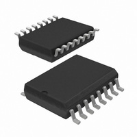
PCA9672D,512 NXP Semiconductors, PCA9672D,512 Datasheet - Page 9

PCA9672D,512
Manufacturer Part Number
PCA9672D,512
Description
IC I/O EXPANDER I2C 8B 16SOIC
Manufacturer
NXP Semiconductors
Datasheet
1.PCA9672PW112.pdf
(27 pages)
Specifications of PCA9672D,512
Interface
I²C
Number Of I /o
8
Interrupt Output
Yes
Frequency - Clock
1MHz
Voltage - Supply
2.3 V ~ 5.5 V
Operating Temperature
-40°C ~ 85°C
Mounting Type
Surface Mount
Package / Case
16-SOIC (0.300", 7.5mm Width)
Includes
POR
Lead Free Status / RoHS Status
Lead free / RoHS Compliant
Other names
935282746512
PCA9672D
PCA9672D
PCA9672D
PCA9672D
NXP Semiconductors
8. I/O programming
PCA9672_2
Product data sheet
8.1 Quasi-bidirectional I/O architecture
8.2 Writing to the port (Output mode)
The PCA9672’s 8 ports (see
input or output ports. Input data is transferred from the ports to the microcontroller in the
Read mode (see
Figure
This quasi-bidirectional I/O can be used as an input or output without the use of a control
signal for data directions. At power-on the I/Os are HIGH. In this mode only a current
source (I
edges into heavily loaded outputs. These devices turn on when an output is written HIGH,
and are switched off by the negative edge of SCL. The I/Os should be HIGH before being
used as inputs. After power-on, as all the I/Os are set HIGH, all of them can be used as
inputs. Any change in setting of the I/Os as either inputs or outputs can be done with the
write mode.
Remark: If a HIGH is applied to an I/O which has been written earlier to LOW, a large
current (I
To write, the master (microcontroller) first addresses the slave device. By setting the last
bit of the byte containing the slave address to logic 0 the write mode is entered. The
PCA9672 acknowledges and the master sends the data byte for P7 to P0 and is
acknowledged by the PCA9672. The 8-bit data is presented on the port lines after it has
been acknowledged by the PCA9672.
The number of data bytes that can be sent successively is not limited. The previous data
is overwritten every time a data byte has been sent.
Fig 11. Device ID field reading
S
START condition
manufacturer name
M7
= 00000000
1
12).
If more than 2 bytes are read, the slave device loops back to the first byte (manufacturer byte)
and keeps sending data until the master generates a ‘no acknowledge’.
OH
M6 M5 M4
OL
device ID address
1
) to V
) will flow to V
1
1
DD
Figure
M3
Remote 8-bit I/O expander for Fm+ I
1
is active. An additional strong pull-up to V
M2 M1 M0
0
0
13). Output data is transmitted to the ports in the Write mode (see
Rev. 02 — 6 July 2007
SS
R/W
0
.
Figure
A
A
acknowledge from one
or several slave(s)
acknowledge
from master
C6
A6
the device to be identified
I
2
category identification
C-bus slave address of
A5 A4 A3 A2 A1 A0 X
C5 C4 C3
2) are entirely independent and can be used either as
= 0000001
C2
C1 C0 F5
don't care
feature identification
acknowledge from
slave to be identified
A
A
acknowledge
from master
= 000011
2
C-bus with interrupt and reset
F4
1
P3 P2 P1
DD
device ID address
1
(I
1
trt(pu)
1
slave to be identified
P0 R2 R1 R0
PCA9672
1
) allows fast rising
acknowledge from
© NXP B.V. 2007. All rights reserved.
revision = 000
no acknowledge
0
from master
0
R/W
1
condition
002aac327
STOP
A
A
9 of 27
P


