MCP23009-E/MG Microchip Technology, MCP23009-E/MG Datasheet
MCP23009-E/MG
Specifications of MCP23009-E/MG


Related parts for MCP23009-E/MG


MCP23009-E/MG Summary of contents
Page 1
... High-speed I C™ interface: (MCP23009) - 100 kHz - 400 kHz - 3.4 MHz • High-speed SPI interface: (MCP23S09 MHz • Single hardware address pin: (MCP23009) - Voltage input to allow up to eight devices on the bus • Configurable interrupt output pins: - Configurable as active-high, active-low or open-drain Block Diagram ...
Page 2
... DD N/C 2 SCL 3 SDA 4 ADDR 5 RESET 6 INT 7 GP0 8 GP1 9 * Includes Exposed Thermal Pad (EP); see Package Types: PDIP/SOIC SCK RESET 7 INT 8 GP0 9 * Includes Exposed Thermal Pad (EP); see DS22121B-page 2 MCP23009 GP7 15 GP6 14 GP5 13 GP4 12 GP3 11 GP2 10 SSOP SCL SDA 4 17 GP7 ADDR 5 GP6 16 ...
Page 3
... I/O expansion for I C bus or SPI applications. The two devices differ only in the serial interface. 2 • MCP23009 - I C interface • MCP23S09 - SPI interface The MCP23X09 consists of multiple 8-bit configuration registers for input, output and polarity selection. The system master can enable the I/Os as either inputs or outputs by writing the I/O configuration bits ...
Page 4
... MCP23009/MCP23S09 1.1 Pin Descriptions 2 TABLE 1- PINOUT DESCRIPTION (MCP23009) 18LD Pin 16LD 20LD PDIP/ Name QFN SSOP SOIC SCL SDA ADDR RESET INT GP0 GP1 GP2 GP3 GP4 GP5 GP6 GP7 16, 2 2,10, 17 11,19 — 17 DS22121B-page 4 Pin Standard Function Type P Power P Ground ...
Page 5
... Bidirectional I/O Pin (5.5 volt tolerant inputs; open-drain outputs). Can be enabled for interrupt on change, and/or internal pull-up resistor — Not connected EP — 17 — Exposed Thermal Pad (EP). Do not electrically connect, Can connect to V © 2009 Microchip Technology Inc. MCP23009/MCP23S09 Standard Function . SS DS22121B-page 5 ...
Page 6
... Start condition and ACK) with the R/W bit equal to a logic one (R/W = 1). The MCP23009 then transmits the data contained in the addressed register. The sequence is ended with the master generating a Stop or Restart condition ...
Page 7
... R/W bit cleared) is then clocked into the device. The opcode is followed by an address and at least one data byte. © 2009 Microchip Technology Inc. MCP23009/MCP23S09 1.3.3.2 SPI Read Operation The SPI read operation is started by lowering CS. The SPI read command (slave address with R/W bit set) is then clocked into the device ...
Page 8
... MCP23009/MCP23S09 2 FIGURE 1-1: MCP23009 I C™ DEVICE PROTOCOL - Start S - Restart Stop P - Write w - Read R - Device opcode OP ADDR - Device address - Data out from MCP23009 D OUT D - Data in to MCP23009 Byte Sequential S OP Byte S OP Sequential S OP DS22121B-page .... W ADDR OUT .... ADDR P Byte and Sequential Write ...
Page 9
... Multi-bit Address Decoder The ADDR pin is used to set the slave address of the 2 MCP23009 (I C only) to allow up to eight devices on the bus using only a single pin. Typically, this would require three pins. The multi-bit Address Decoder employs a basic FLASH ADC architecture (Figure 1-4) ...
Page 10
... MCP23009/MCP23S09 FIGURE 1-3: VOLTAGE AND CODE EXAMPLE Assume A2, A1 opcode ratio = R2/(R1+R2 voltage on ADDR pin V2(min (VDD/8) x %tolerance V2(max (VDD/8) x %tolerance n R2=2n R2=2n R2=2n R2=2n DS22121B-page 10 VDD= 1.8 R1=16-R2 R2/(R1+R2) V2 0.113 15 0.0625 13 0.1875 0.338 11 0.3125 0.563 0.788 9 0.4375 7 0.5625 1.013 1.238 5 0 ...
Page 11
... FIGURE 1-4: FLASH ADC BLOCK DIAGRAM V DD analog_in adc_en gnd © 2009 Microchip Technology Inc. MCP23009/MCP23S09 addr_out[ adc_en adc_en en addr_out[5] adc_en reset addr_out[4] set ' adc_en i2c_clk addr_out[3] adc_en addr_out[2] adc_en addr_out[1] adc_en addr_out[0] adc_en addr[6:0] i2c_addr[2:0] adc_en DS22121B-page 11 ...
Page 12
... ADDRESSING I C DEVICES (MCP23009) 2 The MCP23009 is a slave I C device that supports 7- bit slave addressing, with the read/write bit filling out the control byte. The slave address contains four fixed bits and three user-defined hardware address bits (configured via ADDR pin). ...
Page 13
... FIGURE 1-8: I C™ ADDRESSING REGISTERS Device Opcode The ACKs are provided by the MCP23009. FIGURE 1-9: SPI ADDRESSING REGISTERS Device Opcode © 2009 Microchip Technology Inc. MCP23009/MCP23S09 0 ACK R Register Address 0 R Register Address ACK DS22121B-page 13 ...
Page 14
... MCP23009/MCP23S09 1.5 GPIO Port The GPIO module is a general purpose 8-bit wide bidirectional port. The outputs are open-drain. The GPIO module contains the data ports (GPIOn), internal pull up resistors and the Output Latches (OLATn). The pull up resistors are individually configured and can be enabled when the pin is configured as an input or output ...
Page 15
... GPPUA 06 PU7 PU6 INTFA 07 INT7 INT6 INTCAPA 08 ICP7 ICP6 GPIOA 09 GP7 GP6 OLATA 0A OL7 OL6 © 2009 Microchip Technology Inc. MCP23009/MCP23S09 bit 5 bit 4 bit 3 bit 2 IO5 IO4 IO3 IO2 IP5 IP4 IP3 IP2 GPINT5 GPINT4 GPINT3 GPINT2 DEF5 DEF4 DEF3 DEF2 ...
Page 16
... MCP23009/MCP23S09 1.6.1 I/O DIRECTION REGISTER Controls the direction of the data I/O. When a bit is set, the corresponding pin becomes an input. When a bit is clear, the corresponding pin becomes an output. REGISTER 1-1: IODIR – I/O DIRECTION REGISTER R/W-1 R/W-1 R/W-1 IO7 IO6 IO5 bit 7 ...
Page 17
... IP7:IP0: Controls the polarity inversion of the input pins <7:0> GPIO register bit will reflect the opposite logic state of the input pin 0 = GPIO register bit will reflect the same logic state of the input pin © 2009 Microchip Technology Inc. MCP23009/MCP23S09 R/W-0 R/W-0 R/W-0 ...
Page 18
... MCP23009/MCP23S09 1.6.3 INTERRUPT-ON-CHANGE CONTROL REGISTER The GPINTEN register controls the interrupt-on- change feature for each pin bit is set, the corresponding pin is enabled for interrupt-on-change. The DEFVAL and INTCON registers must also be configured if any pins are enabled for interrupt-on-change. REGISTER 1-3: GPINTEN – INTERRUPT-ON-CHANGE PINS ...
Page 19
... DEF7:DEF0: Sets the compare value for pins configured for interrupt-on-change from defaults <7:0>. Refer to INTCON. If the associated pin level is the opposite from the register bit, an interrupt occurs. Refer to INTCON and GPINTEN. © 2009 Microchip Technology Inc. MCP23009/MCP23S09 R/W-0 R/W-0 R/W-0 DEF4 ...
Page 20
... MCP23009/MCP23S09 1.6.5 INTERRUPT CONTROL REGISTER The INTCON register controls how the associated pin value is compared for the interrupt-on-change feature bit is set, the corresponding I/O pin is compared against the associated bit in the DEFVAL register bit value is clear, the corresponding I/O pin is compared against the previous value ...
Page 21
... Reading INTCAP register clears the interrupt 0 = Reading GPIO register clears the interrupt © 2009 Microchip Technology Inc. MCP23009/MCP23S09 The Interrupt Polarity (INTPOL) sets the polarity of the INT pin. This bit is functional only when the ODR bit is cleared, configuring the INT pin as active push-pull. ...
Page 22
... MCP23009/MCP23S09 1.6.7 PULL-UP RESISTOR CONFIGURATION REGISTER The GPPU register controls the pull-up resistors for the port pins bit is set the corresponding port pin is internally pulled up with an internal resistor. REGISTER 1-7: GPPU – GPIO PULL-UP RESISTOR REGISTER R/W-0 R/W-0 R/W-0 PU7 PU6 ...
Page 23
... Bit is set bit 7-0 INT7:INT0: Reflects the interrupt condition on the port. Will reflect the change only if interrupts are enabled (GPINTEN) <7:0> Pin caused interrupt 0 = Interrupt not pending © 2009 Microchip Technology Inc. MCP23009/MCP23S09 R-0 R-0 R-0 INT4 INT3 INT2 U = Unimplemented bit, read as ‘ ...
Page 24
... MCP23009/MCP23S09 1.6.9 INTERRUPT CAPTURE REGISTER The INTCAP register captures the GPIO port value at the time the interrupt occurred. The register is ‘read only’ and is updated only when an interrupt occurs. The register will remain unchanged until the interrupt is cleared via a read of INTCAP or GPIO. ...
Page 25
... W = Writable bit -n = Value at POR ‘1’ = Bit is set bit 7-0 GP7:GP0: Reflects the logic level on the pins <7:0> Logic-high 0 = Logic-low © 2009 Microchip Technology Inc. MCP23009/MCP23S09 R/W-0 R/W-0 R/W-0 GP4 GP3 GP2 U = Unimplemented bit, read as ‘0’ ‘0’ = Bit is cleared ...
Page 26
... MCP23009/MCP23S09 1.6.11 OUTPUT LATCH REGISTER (OLAT) The OLAT register provides access to the output latches. A read from this register results in a read of the OLAT and not the port itself. A write to this register modifies the output latches that modifies the pins configured as outputs. ...
Page 27
... INTCAP register. Subsequent interrupt conditions on the port will not cause an interrupt to occur as long as the interrupt is not cleared by a read of INTCAP or GPIO. © 2009 Microchip Technology Inc. MCP23009/MCP23S09 1.7.4 CLEARING INTERRUPTS The interrupt will remain active until the INTCAP or GPIO register is read (depending on IOCON.INTCC). ...
Page 28
... MCP23009/MCP23S09 1.7.5 INTERRUPT CONDITIONS There are two possible configurations to cause interrupts (configured via INTCON): 1. Pins configured for interrupt-on-pin-change will cause an interrupt to occur if a pin changes to the opposite state. The default state is reset after an interrupt occurs. For example, an interrupt occurs by an input changing from 1 to ...
Page 29
... This is a stress rating only and functional operation of the device at those or any other conditions above those indicated in the operation listings of this specification is not implied. Exposure to maximum rating conditions for extended periods may affect device reliability. © 2009 Microchip Technology Inc. MCP23009/MCP23S09 ..................................................................................................... -0.3V to +14V (except V and GPIOA/B) ..................................... -0. ...
Page 30
... MCP23009/MCP23S09 2.1 DC CHARACTERISTICS Operating Conditions (unless otherwise indicated): DC Characteristics 1.8V ≤ V Param Characteristic Sym No. D001 Supply Voltage V DD D002 V Start Voltage POR Ensure Power-on Reset D003 V Rise Rate Ensure Power-on Reset D004 Supply Current I DD D005 Standby (Idle) current I DDS Input Low-Voltage ...
Page 31
... POR at device power up POR 34 Tio Output Hi-impedance from Z RESET Low Note 1: This parameter is characterized, not 100% tested. 2: Data in the Typical (“Typ”) column is at 5V, +25°C, unless otherwise stated. © 2009 Microchip Technology Inc. MCP23009/MCP23S09 V DD Pin 1 kΩ 135 ≤ +125° ...
Page 32
... MCP23009/MCP23S09 TABLE 2-2: GP AND INT PINS AC Characteristics Standard Operating Conditions (unless otherwise specified) 1.8V ≤ V ≤ 5.5V at -40°C ≤ Parameter No. Sym Characteristic 50 t Serial data to output valid GPOV 51 t Interrupt pin disable time INTD input change to register valid GPIV 53 t IOC event to INT active ...
Page 33
... This parameter is characterized, not 100% tested. 2: Data in the Typical (“Typ”) column is at 5V, +25°C, unless otherwise stated.. FIGURE 2-4: HARDWARE ADDRESS LATCH TIMING adc_en i2c_addr[2:0] SCL © 2009 Microchip Technology Inc. MCP23009/MCP23S09 ≤ +125° Min Typ Max stable after — 0 — — 50 — ...
Page 34
... MCP23009/MCP23S09 2 FIGURE 2- BUS START/STOP BITS TIMING SCL 91 90 SDA START Condition Note 1: Refer to Figure 2-1 for load conditions. 2 FIGURE 2- BUS DATA TIMING 103 SCL 90 91 SDA In 109 SDA Out Note 1: Refer to Figure 2-1 DS22121B-page 34 100 101 106 107 109 for load conditions. ...
Page 35
... This parameter is characterized, not 100% tested specified from 10 to 400 (pF This parameter is not applicable in high-speed mode (3.4 MHz). © 2009 Microchip Technology Inc. MCP23009/MCP23S09 Operating Conditions (unless otherwise indicated): 1.8V ≤ V ≤ 5.5V at -40°C ≤ T ≤ +125° (SCL, SDA kΩ, C (SCL, SDA) = 135 pF ...
Page 36
... MCP23009/MCP23S09 2 TABLE 2- BUS DATA REQUIREMENTS (SLAVE MODE) (CONTINUED C™ AC Characteristics Param Characteristic No. 109 Output Valid From Clock: 100 kHz mode 400 kHz mode 3.4 MHz mode 110 Bus Free Time: 100 kHz mode 400 kHz mode 3.4 MHz mode Bus Capacitive Loading: 100 kHz and 400 kHz 3 ...
Page 37
... FIGURE 2-8: SPI OUTPUT TIMING SCK 12 SO MSB out SI © 2009 Microchip Technology Inc. MCP23009/MCP23S09 13 don’t care 2 Mode 1,1 Mode 0,0 14 LSB out DS22121B-page 37 ...
Page 38
... MCP23009/MCP23S09 TABLE 2-5: SPI INTERFACE AC CHARACTERISTICS Operating Conditions (unless otherwise indicated): SPI Interface AC Characteristics 1.8V ≤ V Param Characteristic No. Clock Frequency 1 CS Setup Time 2 CS Hold Time 3 CS Disable Time 4 Data Setup Time 5 Data Hold Time 6 CLK Rise Time 7 CLK Fall Time ...
Page 39
... Microchip Technology Inc. MCP23009/MCP23S09 Example 239 E919 256 Example: MCP23009 e 3 E/P^^ 0919256 Example: MCP23009 e 3 E/SO^^ 0919 256 Example: MCP23009 e 3 E/SS^^ 0919 256 DS22121B-page 39 ...
Page 40
... MCP23009/MCP23S09 Note: For the most current package drawings, please see the Microchip Packaging Specification located at http://www.microchip.com/packaging DS22121B-page 40 © 2009 Microchip Technology Inc. ...
Page 41
... Note: For the most current package drawings, please see the Microchip Packaging Specification located at http://www.microchip.com/packaging © 2009 Microchip Technology Inc. MCP23009/MCP23S09 DS22121B-page 41 ...
Page 42
... MCP23009/MCP23S09 /HDG 3ODVWLF 'XDO ,Q /LQH 3 ± 1RWH N NOTE 1RWHV DS22121B-page 42 PLO %RG\ >3', © 2009 Microchip Technology Inc. ...
Page 43
... D N NOTE 1RWHV © 2009 Microchip Technology Inc. MCP23009/MCP23S09 PP %RG\ >62,& α φ A2 β DS22121B-page 43 ...
Page 44
... MCP23009/MCP23S09 /HDG 3ODVWLF 6KULQN 6PDOO 2XWOLQH 66 ± 1RWH D N NOTE 1RWHV DS22121B-page 44 PP %RG\ >6623 © 2009 Microchip Technology Inc. φ L ...
Page 45
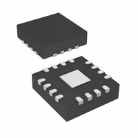
... APPENDIX A: REVISION HISTORY Revision B (May 2009) The following is the list of modifications: 1. Added the 3x3 QFN package (MG package marking). 2. Updated Revision History. Revision A (December 2008) • Original Release of this Document. © 2009 Microchip Technology Inc. MCP23009/MCP23S09 DS22121B-page 45 ...
Page 46
... MCP23009/MCP23S09 NOTES: DS22121B-page 46 © 2009 Microchip Technology Inc. ...
Page 47
... MCP23009-E/SO: Extended Temp MCP23009T-E/SO: Tape and Reel, C™ Interface 2 C Interface d) MCP23009-E/SS: e) MCP23009T-E/SS: Tape and Reel, f) MCP23009-E/MG: Extended Temp., a) MCP23S09-E/P: b) MCP23S09-E/SO: Extended Temp., c) MCP23S09T-E/SO: Tape and Reel, d) MCP23S09T-E/MG: Tape and Reel, Extended Temp., 18LD PDIP package. 18LD SOIC package. Extended Temp., 18LD SOIC package ...
Page 48
... MCP23009/MCP23S09 NOTES: DS22121B-page 48 © 2009 Microchip Technology Inc. ...
Page 49
... PowerInfo, PowerMate, PowerTool, REAL ICE, rfLAB, Select Mode, Total Endurance, TSHARC, WiperLock and ZENA are trademarks of Microchip Technology Incorporated in the U.S.A. and other countries. SQTP is a service mark of Microchip Technology Incorporated in the U.S.A. All other trademarks mentioned herein are property of their respective companies. ...
Page 50
... Fax: 886-3-6578-370 Taiwan - Kaohsiung Tel: 886-7-536-4818 Fax: 886-7-536-4803 Taiwan - Taipei Tel: 886-2-2500-6610 Fax: 886-2-2508-0102 Thailand - Bangkok Tel: 66-2-694-1351 Fax: 66-2-694-1350 © 2009 Microchip Technology Inc. EUROPE Austria - Wels Tel: 43-7242-2244-39 Fax: 43-7242-2244-393 Denmark - Copenhagen Tel: 45-4450-2828 Fax: 45-4485-2829 France - Paris Tel: 33-1-69-53-63-20 ...