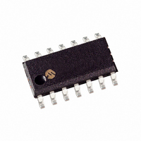
MCP25055-I/SL Microchip Technology, MCP25055-I/SL Datasheet - Page 21

MCP25055-I/SL
Manufacturer Part Number
MCP25055-I/SL
Description
IC I/O EXPANDER CAN 8B 14SOIC
Manufacturer
Microchip Technology
Specifications of MCP25055-I/SL
Package / Case
14-SOIC (3.9mm Width), 14-SOL
Interface
1-Wire, CAN
Number Of I /o
8
Interrupt Output
No
Frequency - Clock
4MHz
Voltage - Supply
2.7 V ~ 5.5 V
Operating Temperature
-40°C ~ 85°C
Mounting Type
Surface Mount
Includes
ADC, Memory, PWM
Product
Controller Area Network (CAN)
Number Of Transceivers
1
Data Rate
1 Mbps
Supply Voltage (max)
5.5 V
Supply Voltage (min)
2.7 V
Supply Current (max)
20 mA
Maximum Operating Temperature
+ 150 C
Minimum Operating Temperature
- 65 C
Mounting Style
SMD/SMT
Lead Free Status / RoHS Status
Lead free / RoHS Compliant
Other names
MCP25055I/SL
Available stocks
Company
Part Number
Manufacturer
Quantity
Price
Company:
Part Number:
MCP25055-I/SL
Manufacturer:
Microchip Technology
Quantity:
135
Company:
Part Number:
MCP25055-I/SL
Manufacturer:
Microchip Technology
Quantity:
184
4.0
4.1
The following sections describe the events/actions of
the MCP2502X/5X during normal power-up and
operation.
4.1.1
The MCP2502X/5X goes through a sequence of events
at power-on reset (POR) in order to load the
programmed configuration and insure that errors are
not introduced on the bus. During this time, the device
is prevented from generating a low condition on the
TXCAN pin. The TXCAN pin must remain high from
power-on until the device goes on bus.
Operational Mode at Power-On
The MCP2502X/5X initially powers up in Configuration
mode. While in this mode, the MCP2502X/5X will be
prevented from sending or receiving messages via the
CAN interface. The ADC and PWM peripherals are
disabled while in this mode.
Self-Configuration
Once the MCP2502X/5X is out of reset, it will perform
a
transferring the contents of the EPROM array to the
corresponding locations within the SRAM array. In
addition, the checksum of the data written to SRAM will
be compared to a pre-programmed value as a test of
valid data.
Going On Bus
Once the self-configuration cycle has successfully
completed, the MCP2502X/5X switches to Listen-only
mode. It will remain in this mode until an error-free CAN
message is detected. This is done to ensure that the
device is at the correct bus rate for the system.
Once the device detects an error-free message, it waits
for CAN bus idle before switching to Normal mode. This
prevents it from going on bus in the middle of another
node’s transmission and generating an error frame.
Alternately, the MCP2505X may directly enter Normal
mode (without first entering Listen-only Mode) after
completing its self-configuration. This is configured by
the user via a control bit (OPTREG2.PUNRM).
Once the MCP2502X/5X enters Normal mode, it is
ready to send/receive messages via the CAN interface.
At this point the ADC and PWM peripherals are
operational, if enabled.
© 2007 Microchip Technology Inc.
self-configuration.
DEVICE OPERATION
Power-Up Sequence
POWER-ON RESET
This
is
accomplished
by
Scheduled Transmissions
Once the MCP2502X/5X has gone on bus it will
transmit the On Bus message once, regardless of
whether enabled or not. This message notifies the
network of the MCP2502X/5X’s presence. The On Bus
message will (if enabled STCON.STEN) repeat at a
frequency
(Register 4-1).
This message can also be configured to send the
“Read A/D Register” data bytes along with the
predefined
STCON.STMS = 1.
4.2
The MCP2502X/5X uses the global mask (RXMASK),
two filters (RXF0 and RXF1) and two receive buffers
(RB0 and RB1) to determine if a received message
should be acted upon. There are 16 functions that can
be performed by the MCP2502X/5X based on received
messages (see Table 4-1).These functions allow the
device to not only be accessed for Information
Request/Input/Output operations, but also to be
reconfigured via the CAN bus, if necessary.
4.3
There are three types of messages that are used to
implement the functions of Table 4-1.
1.
2.
3.
Note:
Note:
Note:
Information Request Messages (IRM)
- Received by the MCP2502X/5X.
Output Messages - Transmitted from the
MCP2502X/5X as a response to IRMs.
Input Messages - Received by the MCP2502X/
5X and used to modify registers.
Message Functions
Message Types
The first On Bus message sent after
power-up will NOT send the “Read A/D
Register” data bytes, regardless of the
STCON.STMS value.
If the MCP2502X/5X enters SLEEP mode,
the scheduled transmissions will cease
until the device wakes up again. This
implies that SLEEP mode has priority over
scheduled transmissions.
Information Request Messages (IRMs)
and Input messages are both input
messages to the MCP2502X/5X. IRMs are
received into receive buffer 0 and input
messages are received into receive buffer
1. This must be taken into account while
configuring the acceptance filters.
determined
identifier
MCP2502X/5X
by
in
the
TXID2
DS21664D-page 21
STCON
by
register
setting


