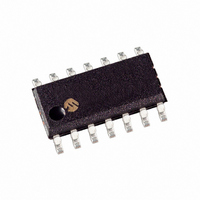
MCP25055-I/SL Microchip Technology, MCP25055-I/SL Datasheet - Page 22

MCP25055-I/SL
Manufacturer Part Number
MCP25055-I/SL
Description
IC I/O EXPANDER CAN 8B 14SOIC
Manufacturer
Microchip Technology
Specifications of MCP25055-I/SL
Package / Case
14-SOIC (3.9mm Width), 14-SOL
Interface
1-Wire, CAN
Number Of I /o
8
Interrupt Output
No
Frequency - Clock
4MHz
Voltage - Supply
2.7 V ~ 5.5 V
Operating Temperature
-40°C ~ 85°C
Mounting Type
Surface Mount
Includes
ADC, Memory, PWM
Product
Controller Area Network (CAN)
Number Of Transceivers
1
Data Rate
1 Mbps
Supply Voltage (max)
5.5 V
Supply Voltage (min)
2.7 V
Supply Current (max)
20 mA
Maximum Operating Temperature
+ 150 C
Minimum Operating Temperature
- 65 C
Mounting Style
SMD/SMT
Lead Free Status / RoHS Status
Lead free / RoHS Compliant
Other names
MCP25055I/SL
Available stocks
Company
Part Number
Manufacturer
Quantity
Price
Company:
Part Number:
MCP25055-I/SL
Manufacturer:
Microchip Technology
Quantity:
135
Company:
Part Number:
MCP25055-I/SL
Manufacturer:
Microchip Technology
Quantity:
184
MCP2502X/5X
4.3.1
Information Request Messages (IRM) are messages
that the MCP2502X/5X receives into Receive Buffer 0
(matches Filter 0) and then responds to by transmitting
a message (output message) containing the requested
data.
IRMs can be implemented as either a Remote Transfer
Request (RTR) or a Data Frame message by
configuring the MTYPE bit in the OPTREG2 register.
TABLE 4-1:
DS21664D-page 22
Read A/D
Registers
Read Control
Registers
Read Configura-
tion Registers
Read CAN
error states
Read PWM
Configuration
Read User
Registers 1
Read User
Registers 2
Read Register*
Write Register
Write TX Message
ID0 (TXID0)
Write TX Message
ID1 (TXID1)
Write TX Message
ID2 (TXID2)
Write I/O
Configuration
Registers
Write RX Mask
Write RX Filter0
Write RX Filter1
* The Read Register command is available when using
extended message format only. Not available with
standard message format.
Name
INFORMATION REQUEST
MESSAGES
MESSAGE FUNCTION
Transmits a single message containing
the current state of the analog and I/O
registers, including the configuration
Transmits several control registers not
included in other messages
Transmits the contents of many of the
configuration registers
Transmits the error flag register and
the error counts
Transmits the registers associated with
the PWM modules
Transmits the values in bytes 0 - 7 of
the user memory
Transmits the values in bytes 8 -15 of
the user memory
Transmits a single byte containing the
value in an addressed user memory
register
Uses a mask to write a value to an
addressed register
Writes the identifiers to a specified
value
Writes the identifiers to a specified
value
Writes the identifiers to a specified
value
Writes specified values to the three
IOCON registers
specified value
Changes the specified filter to the
specified value
Changes the specified filter to the
specified value
Changes the receive mask to the
Description
4.3.1.1
When
(OPTREG2.MTYPE) and a node in the system wants
information from the MCP2502X/5X, it has to send a
remote frame on the bus. The identifier for the remote
frame must be such that it will be accepted through the
MCP2502X/5X’s mask/filter process (using RXF0). The
RTR message type (remote frames) is the default
configuration (MTYPE bit = 0).
Information Request “RTR” messages must not only
meet the RXMASK/RXF0 criteria but must also have
the RTR bit of the CAN ID set (since the filter registers
do not contain an explicit RTR bit). If a message passes
the mask/filter process and the RTR bit is a ‘0’, that
message will be ignored.
Once the MCP2502X/5X has received a remote frame,
it will determine the function to be performed based
upon the three LSb’s (RXB0SIDL.SID2:SID0 for
standard messages and RXB0EID0.EID2:EID0 for
extended messages) of the received remote frame.
Additionally, a predefined Data Length Code (DLC)
must be sent to signify the number of data bytes that
the MCP2502X/5X must return in it’s output message
(see Table 4-2 and Table 4-3).
4.3.1.2
When a non-RTR (or data frame) message type is
selected and a node in the system wants information
from the MCP2502X/5X, it sends an Information
Request in the form of a data frame. The identifier for
this request must be such that it will be accepted
through the MCP2502X/5X’s mask/filter process (using
RXF0).
Information request messages in the data frame format
must not only meet the RXMASK/RXF0 criteria, but
must also have the RTR bit of the CAN ID cleared
(since the filter registers do not contain an explicit RTR
bit). If a message passes the mask/filter process and
the RTR bit is a ‘1’, that message will be ignored.
Once the MCP2502X/5X has received a data frame
information request, it will determine the function to be
performed
(RXB0SIDL.SID2:SID0 for standard messages and
RXB0EID0.EID2:EID0 for extended messages) of the
received data frame. Also, Bit 3 of the received
message ID must be set to a ‘1’.
In addition, the data length code (DLC) must be set to
a zero. Refer to Table 4-2 and Table 4-3 for more
information.
Regardless of the message format, all messages
except the Read Register message can use either
standard or extended identifiers. The Read Register
message has one additional requirement; it must be an
extended identifier. This is discussed in more detail in
Table 4-1 and Table 4-3 for more information.
RTR
RTR Message Type
Data Frame Message Type
based
message
© 2007 Microchip Technology Inc.
upon
types
the
are
three
selected
LSb’s


