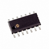
MCP25055-I/SL Microchip Technology, MCP25055-I/SL Datasheet - Page 3

MCP25055-I/SL
Manufacturer Part Number
MCP25055-I/SL
Description
IC I/O EXPANDER CAN 8B 14SOIC
Manufacturer
Microchip Technology
Specifications of MCP25055-I/SL
Package / Case
14-SOIC (3.9mm Width), 14-SOL
Interface
1-Wire, CAN
Number Of I /o
8
Interrupt Output
No
Frequency - Clock
4MHz
Voltage - Supply
2.7 V ~ 5.5 V
Operating Temperature
-40°C ~ 85°C
Mounting Type
Surface Mount
Includes
ADC, Memory, PWM
Product
Controller Area Network (CAN)
Number Of Transceivers
1
Data Rate
1 Mbps
Supply Voltage (max)
5.5 V
Supply Voltage (min)
2.7 V
Supply Current (max)
20 mA
Maximum Operating Temperature
+ 150 C
Minimum Operating Temperature
- 65 C
Mounting Style
SMD/SMT
Lead Free Status / RoHS Status
Lead free / RoHS Compliant
Other names
MCP25055I/SL
Available stocks
Company
Part Number
Manufacturer
Quantity
Price
Company:
Part Number:
MCP25055-I/SL
Manufacturer:
Microchip Technology
Quantity:
135
Company:
Part Number:
MCP25055-I/SL
Manufacturer:
Microchip Technology
Quantity:
184
1.0
This document contains device-specific information on
the MCP2502X/5X family of CAN I/O expanders. The
CAN protocol is not discussed in depth in this
document. Additional information on the CAN protocol
can be found in the CAN specification, as defined by
Robert Bosch GmbH.
FIGURE 1-1:
TABLE 1-1:
© 2007 Microchip Technology Inc.
GP0/AN0 *
GP1/AN1 *
GP2/AN2/PWM2 *
GP3/AN3/PWM3 *
GP4/V
GP5/V
V
OSC1/CLKIN
OSC2
GP6/CLKOUT
GP7/RST/V
RXCAN
TXCAN/TXRXCAN
V
* Only the MCP2505X devices have the A/D module.
OSC2/CLKOUT
OSC1/CLKIN
SS
DD
* Only the MCP2505X devices have the A/D module.
REF
REF
Name
Pin
DEVICE OVERVIEW
-
+
PP
PINOUT DESCRIPTION
Number
MCP2502X/5X BLOCK DIAGRAM
Generation
Pin
10
12
13
14
Memory
11
Timing
1
2
3
4
5
6
7
8
9
User
PWM2
Bidirectional I/O pin, TTL input buffer
Bidirectional I/O pin, TTL input buffer
Bidirectional I/O pin, TTL input buffer
Bidirectional I/O pin, TTL input buffer
Bidirectional I/O pin, TTL input buffer
Bidirectional I/O pin, TTL input buffer
Ground
External oscillator input
External oscillator output
Bidirectional I/O pin, TTL input buffer
Input pin, TTL input buffer
CAN data receive input
CAN data transmit output
Power
PWM1
Standard
Function
State Machine
Control Logic
and
Figure 1-1 is the block diagram of the MCP2502X/5X
and Table 1-1 is the pinout description.
The following sections detail the modules as listed in
Figure 1-1.
A/D
*
Analog input channel
Analog input channel
Analog input/PWM output
Analog input/PWM output
External V
External V
None
External clock input
None
CLKOUT output
External Reset input
Not connected for 1-wire
CAN TX and RX for 1-wire
operation (MCP250X5)
None
Alternate
Function
REF
REF
MCP2502X/5X
-
input
GPIO
Protocol
Engine
CAN
GP0/AN0
GP1/AN1
GP2/AN2/PWM1
GP3/AN3/PWM2
GP4/V
GP5/V
GP6/CLKOUT
GP7RST/V
Mode Function
Programming
DS21664D-page 3
TXCAN/
TXRXCAN
RXCAN
Ground
Power
REF
REF
Clock
None
None
None
None
None
None
None
None
None
Data
Vpp
-
+
PP


