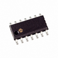
MCP25055-I/SL Microchip Technology, MCP25055-I/SL Datasheet - Page 31

MCP25055-I/SL
Manufacturer Part Number
MCP25055-I/SL
Description
IC I/O EXPANDER CAN 8B 14SOIC
Manufacturer
Microchip Technology
Specifications of MCP25055-I/SL
Package / Case
14-SOIC (3.9mm Width), 14-SOL
Interface
1-Wire, CAN
Number Of I /o
8
Interrupt Output
No
Frequency - Clock
4MHz
Voltage - Supply
2.7 V ~ 5.5 V
Operating Temperature
-40°C ~ 85°C
Mounting Type
Surface Mount
Includes
ADC, Memory, PWM
Product
Controller Area Network (CAN)
Number Of Transceivers
1
Data Rate
1 Mbps
Supply Voltage (max)
5.5 V
Supply Voltage (min)
2.7 V
Supply Current (max)
20 mA
Maximum Operating Temperature
+ 150 C
Minimum Operating Temperature
- 65 C
Mounting Style
SMD/SMT
Lead Free Status / RoHS Status
Lead free / RoHS Compliant
Other names
MCP25055I/SL
Available stocks
Company
Part Number
Manufacturer
Quantity
Price
Company:
Part Number:
MCP25055-I/SL
Manufacturer:
Microchip Technology
Quantity:
135
Company:
Part Number:
MCP25055-I/SL
Manufacturer:
Microchip Technology
Quantity:
184
5.0
5.1
The MCP2502X/5X has eight general-purpose input/
output pins (GP0 to GP7), collectively labeled GPIO. All
GPIO port pins have TTL input levels and full CMOS
output drivers, with the exception of GP7, which is input
only. Pins GP6:GP0 can be individually configured as
input or output via the GPDDR register.
Each of the GPIO pins has a weak internal pull-up
resistor. A single control bit (OPTREG.GPPU) can turn
on/off all the pull-ups. The weak pull-up is automatically
turned off when the port pin is configured as an output.
The pull-ups are disabled during a Power-on Reset.
All pins are multiplexed with an alternate function,
including analog-to-digital conversion on up to four of
the GPIO pins, analog V
outputs up to two pins, clock-out function and external
reset. The operation of each pin is selected by clearing,
or setting, control bits in various control registers. GPIO
pin functions are summarized in Table 5-1.
TABLE 5-1:
© 2007 Microchip Technology Inc.
GP0/AN0
GP1/AN1
GP2/AN2/PWM2
GP3/AN3/PWM3
GP4/V
GP5/V
GP6/CLKOUT
GP7/nRST/V
Note:
Name
REF
REF
GPIO MODULE
Description
-
+
The GPDDR register controls the direction
of the GPIO pins, even when they are
being used as analog inputs. The user
must ensure that the bits in the GPDDR
register are maintained set (input) when
using them as analog inputs.
PP
GPIO FUNCTIONS
bit0 I/O or analog input
bit1 I/O or analog input
bit2 I/O, analog input
bit3 I/O, analog input
bit4 I/O or analog voltage
bit5 I/O or analog voltage
bit6 I/O or Clock output
bit7 Input, external reset input
Bit
#
REF
or PWM out
or PWM out
reference
reference
or programming voltage
input
inputs up to two pins, PWM
Function
5.2
All GPIO pins have a digital input edge detection
feature that will automatically transmit a message when
an edge with the proper polarity occurs on any of the
digital inputs. Only pins configured as inputs and
enabled for this function via control register IOINTPO
will perform this operation.
Three control registers are associated with this
function. An enable pin for each GPIO pin resides in the
IOINTEN register. When a bit is set to a '1', the
corresponding GPIO pin is enabled to generate a
transmit-on-change message (TXID2) when an edge of
specified polarity occurs.
The digital edge detection function on a GPIO pin
configured as a digital input is edge triggered. A rising-
edge will generate a transmission if the corresponding
bit in the IOINTPO register is set. A falling-edge will
generate a transmission if the bit is cleared. When a
valid edge appears on the enabled GPIO pin, CAN
message TXID2 is initiated.
The edge-detection function on any given GPIO pin
(configured as a digital input) can wake up the
processor from SLEEP if the corresponding interrupt
enable bit in the IOINTEN register was set prior to
going into SLEEP mode. If a wake-up from SLEEP is
caused in this manner, the device will immediately
initiate a transmit message (TXID2).
Note:
Digital Input Edge Detection
Refer to Section 7.4 “A/D Threshold
Detection” for information regarding A/D
channels.
MCP2502X/5X
DS21664D-page 31


