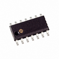
MCP25055T-I/SL Microchip Technology, MCP25055T-I/SL Datasheet - Page 38

MCP25055T-I/SL
Manufacturer Part Number
MCP25055T-I/SL
Description
IC I/O EXPANDER CAN 8B 14SOIC
Manufacturer
Microchip Technology
Specifications of MCP25055T-I/SL
Package / Case
14-SOIC (3.9mm Width), 14-SOL
Interface
1-Wire, CAN
Number Of I /o
8
Interrupt Output
No
Frequency - Clock
4MHz
Voltage - Supply
2.7 V ~ 5.5 V
Operating Temperature
-40°C ~ 85°C
Mounting Type
Surface Mount
Includes
ADC, Memory, PWM
Product
Controller Area Network (CAN)
Number Of Transceivers
1
Data Rate
1 Mbps
Supply Voltage (max)
5.5 V
Supply Voltage (min)
2.7 V
Supply Current (max)
20 mA
Maximum Operating Temperature
+ 150 C
Minimum Operating Temperature
- 65 C
Mounting Style
SMD/SMT
Lead Free Status / RoHS Status
Lead free / RoHS Compliant
Other names
MCP25055TI/SL
Available stocks
Company
Part Number
Manufacturer
Quantity
Price
Company:
Part Number:
MCP25055T-I/SL
Manufacturer:
MICROCHIP
Quantity:
12 000
MCP2502X/5X
6.3.2
The PWM duty cycle is specified by writing to the
PWMnDCH and TnCON registers. Up to 10-bit
resolution is available. The PWMnDCH contains the
eight MSb’s, while the TnCON register contains the two
LSb’s.
PWM1DCH:T1CON<1:0> for PWM Module 1 and
PWM2DCH:T2CON<1:0> for PWM Module 2.
The following equation is used to calculate the PMW
duty cycle:
PWMnDCH can be written to at any time, but the duty
cycle value is not latched into PWMnDBH until after a
match between PRn and TMRn occurs (i.e., the period
is complete).
The PWMnDBH register and 2-bit internal latch are
used to double-buffer the PWM duty cycle. This
double-buffering is essential for glitchless PWM
operation.
TABLE 6-1:
REGISTER 6-1:
REGISTER 6-2:
DS21664D-page 38
Timer Prescaler (1, 4, 16)
PRn Value
Maximum Resolution (bits)
PWMDC
This
PWM Frequency
bit 7-0
bit 7-0
PWM DUTY CYCLE
=
(
10-bit
PWMnDC
PWM FREQUENCIES AND RESOLUTIONS AT 20 MHZ
PWM1 DUTY CYCLE REGISTER MSB (PWM1DCH)
PWM2 DUTY CYCLE REGISTER MSB (PWM2DCH)
DC1B9:DC1B2: Most Significant PWM0 Duty Cycle bits
Legend:
R = Readable bit
- n = Value at POR
DC2B9:DC2B2: Most Significant PWM2 Duty Cycle bits
Legend:
R = Readable bit
- n = Value at POR
bit 7
bit 7
value
DC1B9
DC2B9
R/W-x
R/W-x
)
*T
OSC
is
*TMRn (prescale)
DC1B8
DC2B8
represented
R/W-x
R/W-x
1.22 kHz
0xFF
16
10
DC1B7
DC2B7
R/W-x
R/W-x
W = Writable bit
W = Writable bit
‘1’ = Bit is set
‘1’ = Bit is set
by
4.88 kHz
0xFF
10
4
DC1B6
DC2B6
R/W-x
R/W-x
When the PWMnDBH and 2-bit latch match TMRn
concatenated with an internal 2-bit Q clock or 2 bits of
the TMRn prescaler, the PWM output pin is cleared.
Maximum PWM resolution (bits) for a given PWM
frequency is equal to:
In order to achieve higher resolution, the PWM
frequency must be decreased. In order to achieve
higher PWM frequency, the resolution must be
decreased. Table 6-1 lists example PWM frequencies
and resolutions for F
and PRn values are also shown.
Note:
19.53 kHz
0xFF
10
1
DC1B5
DC2B5
U = Unimplemented bit, read as ‘0’
‘0’ = Bit is cleared
U = Unimplemented bit, read as ‘0’
‘0’ = Bit is cleared
log F
R/W-x
R/W-x
If the PWM duty cycle value is longer than
the PWM period (PWM duty cycle
cleared.
= 100%), the PWM output pin will not be
(
(
OSC
78.12 kHz 156.30 kHz 208.30 kHz
0x3F
)
1
8
⁄
OSC
DC1B4
DC2B4
(
R/W-x
R/W-x
Fpwm
© 2007 Microchip Technology Inc.
= 20 MHz. TMRn prescaler
)
)
⁄
x = Bit is unknown
x = Bit is unknown
0x1F
(
DC1B3
DC2B3
log 2 ( )bits
R/W-x
R/W-x
1
7
)
DC1B2
DC2B2
0x17
R/W-x
R/W-x
5.5
1
bit 0
bit 0


