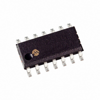
MCP25055T-I/SL Microchip Technology, MCP25055T-I/SL Datasheet - Page 48

MCP25055T-I/SL
Manufacturer Part Number
MCP25055T-I/SL
Description
IC I/O EXPANDER CAN 8B 14SOIC
Manufacturer
Microchip Technology
Specifications of MCP25055T-I/SL
Package / Case
14-SOIC (3.9mm Width), 14-SOL
Interface
1-Wire, CAN
Number Of I /o
8
Interrupt Output
No
Frequency - Clock
4MHz
Voltage - Supply
2.7 V ~ 5.5 V
Operating Temperature
-40°C ~ 85°C
Mounting Type
Surface Mount
Includes
ADC, Memory, PWM
Product
Controller Area Network (CAN)
Number Of Transceivers
1
Data Rate
1 Mbps
Supply Voltage (max)
5.5 V
Supply Voltage (min)
2.7 V
Supply Current (max)
20 mA
Maximum Operating Temperature
+ 150 C
Minimum Operating Temperature
- 65 C
Mounting Style
SMD/SMT
Lead Free Status / RoHS Status
Lead free / RoHS Compliant
Other names
MCP25055TI/SL
Available stocks
Company
Part Number
Manufacturer
Quantity
Price
Company:
Part Number:
MCP25055T-I/SL
Manufacturer:
MICROCHIP
Quantity:
12 000
MCP2502X/5X
REGISTER 8-1:
8.4
The MCP2502X/5X differentiates between two kinds of
reset:
• Power-on Reset (POR)
• External RST reset
Some registers are not affected in any reset condition.
Their status is unknown on POR and unchanged in any
other reset. Most other registers are reset to a reset
state on Power-on Reset (POR), on RST and on RST
during SLEEP. They are not affected by a wake-up from
SLEEP, which is viewed as the resumption of normal
operation. A simplified block diagram of the on-chip
reset circuit is shown in Figure 8-3. The MCP2502X/5X
has a RST noise filter in the RST reset path. The filter
will detect and ignore small pulses.
DS21664D-page 48
bit 13
U-0
—
Reset
bit 13-11
bit 10-3
bit 2
bit 1-0
U-0
—
CONFIGURATION REGISTER
Unimplemented: Read as '0'
Reserved: do not attempt to modify
RSTEN: Enable RST input on GP7
1 = RST input Enabled
0 = RST input Disabled
F
11 = HS oscillator
10 = Reserved for Test (EC oscillator)
01 = XT oscillator
00 = LP oscillator
Legend:
R = Readable bit
- n = Value at POR
bit 7
OSC
R/W-x
R/W-x
R
1:F
R
OSC
0: Oscillator Selection bits
R/W-x
R/W-x
R
R
R/W-x
R/W-x
R
W = Writable bit
‘1’ = Bit is set
R
R/W-x
R/W-x
R
8.4.1
A Power-on Reset pulse is generated on-chip when
V
RST input on the GP7 pin is selected, the RST pin may
be tied through a series resistor to V
need for external RC components usually required for
a Power-on Reset. A maximum rise time for V
specified in Section 9.0 “Electrical Characteristics”
of this document.
When the device starts normal operation (exits the
reset condition), device operating parameters (voltage,
frequency, temperature, etc.) must be met to ensure
proper operation. For additional information, refer to
AN607, “Power-up Troubleshooting”, DS00607).
R
DD
bit 8
rise is detected (in the range of 1.5V to 2.1V). If the
U = Unimplemented bit, read as ‘0’
‘0’ = Bit is cleared
R/W-x
POWER-ON RESET
R
RSTEN
R/W
© 2007 Microchip Technology Inc.
x = Bit is unknown
FOSC1
R/W
DD
, eliminating the
FOSC0
R/W
DD
bit 0
is


