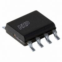
PCA9515AD,112 NXP Semiconductors, PCA9515AD,112 Datasheet - Page 13

PCA9515AD,112
Manufacturer Part Number
PCA9515AD,112
Description
IC I2C BUS REPEATER 8-SOIC
Manufacturer
NXP Semiconductors
Type
Repeaterr
Datasheet
1.PCA9515ADP118.pdf
(18 pages)
Specifications of PCA9515AD,112
Tx/rx Type
I²C Logic
Delay Time
113ns
Capacitance - Input
6pF
Voltage - Supply
2.3 V ~ 3.6 V
Current - Supply
800µA
Mounting Type
Surface Mount
Package / Case
8-SOIC (3.9mm Width)
Operating Temperature (min)
-40C
Operating Temperature Classification
Industrial
Operating Temperature (max)
85C
Package Type
SO
Rad Hardened
No
For Use With
OM6285 - EVAL BOARD I2C-2002-1A568-4002 - DEMO BOARD I2C
Lead Free Status / RoHS Status
Lead free / RoHS Compliant
Other names
568-1753-5
935276766112
PCA9515AD
PCA9515AD
935276766112
PCA9515AD
PCA9515AD
NXP Semiconductors
13. Soldering of SMD packages
PCA9515A_4
Product data sheet
13.1 Introduction to soldering
13.2 Wave and reflow soldering
13.3 Wave soldering
This text provides a very brief insight into a complex technology. A more in-depth account
of soldering ICs can be found in Application Note AN10365 “Surface mount reflow
soldering description” .
Soldering is one of the most common methods through which packages are attached to
Printed Circuit Boards (PCBs), to form electrical circuits. The soldered joint provides both
the mechanical and the electrical connection. There is no single soldering method that is
ideal for all IC packages. Wave soldering is often preferred when through-hole and
Surface Mount Devices (SMDs) are mixed on one printed wiring board; however, it is not
suitable for fine pitch SMDs. Reflow soldering is ideal for the small pitches and high
densities that come with increased miniaturization.
Wave soldering is a joining technology in which the joints are made by solder coming from
a standing wave of liquid solder. The wave soldering process is suitable for the following:
Not all SMDs can be wave soldered. Packages with solder balls, and some leadless
packages which have solder lands underneath the body, cannot be wave soldered. Also,
leaded SMDs with leads having a pitch smaller than ~0.6 mm cannot be wave soldered,
due to an increased probability of bridging.
The reflow soldering process involves applying solder paste to a board, followed by
component placement and exposure to a temperature profile. Leaded packages,
packages with solder balls, and leadless packages are all reflow solderable.
Key characteristics in both wave and reflow soldering are:
Key characteristics in wave soldering are:
•
•
•
•
•
•
•
•
•
•
Through-hole components
Leaded or leadless SMDs, which are glued to the surface of the printed circuit board
Board specifications, including the board finish, solder masks and vias
Package footprints, including solder thieves and orientation
The moisture sensitivity level of the packages
Package placement
Inspection and repair
Lead-free soldering versus SnPb soldering
Process issues, such as application of adhesive and flux, clinching of leads, board
transport, the solder wave parameters, and the time during which components are
exposed to the wave
Solder bath specifications, including temperature and impurities
Rev. 04 — 11 April 2008
PCA9515A
© NXP B.V. 2008. All rights reserved.
I
2
C-bus repeater
13 of 18


