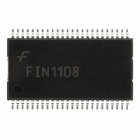
FIN1108MTDX Fairchild Semiconductor, FIN1108MTDX Datasheet

FIN1108MTDX
Specifications of FIN1108MTDX
FIN1108MTDXTR
Available stocks
Related parts for FIN1108MTDX
FIN1108MTDX Summary of contents
Page 1
... V Reference Output BB Ordering Information Operating Part Number Temperature Range FIN1108MTD -40 to +85°C FIN1108MTDX -40 to +85°C © 2002 Fairchild Semiconductor Corporation FIN1108 • Rev. 1.0.4 Descriptions This eight-port repeater is designed for high-speed interconnects utilizing Signaling (LVDS) technology. The FIN1108 accepts and outputs LVDS levels with a ...
Page 2
... Pin Configuration Pin Definitions Pin # 1,2,23,37,36 3 4,7,8,11,14,17,18,21 R 5,6,9,10,15,16,19,20 R IN1+ 12,25,26,47, 28,31,32,35,38,41,42,45 D 29,30,33,34,39,40,43,44 46 © 2002 Fairchild Semiconductor Corporation FIN1108 • Rev. 1.0.4 Figure 1. Pin Configuration Name GND / IN1- IN2- IN3- IN5- IN6- IN7- IN8 IN2+ IN3+ IN5+ IN6+ IN7+ IN8+ VCC EN /EN ...
Page 3
... Table 1. Function Table EN /EN XX HIGH LOW HIGH LOW HIGH LOW Don’t Care HIGH LOW Don’t Care © 2002 Fairchild Semiconductor Corporation FIN1108 • Rev. 1.0.4 Figure 2. Functional Diagram Inputs D D IN+ IN- HIGH LOW LOW HIGH Fail-Safe Don’t Care Don’ ...
Page 4
... Absolute Maximum Ratings. Symbol Parameter V Supply Voltage CC ⏐V ⏐ Magnitude of Differential Voltage ID V Common Mode Voltage Range IC T Operating Temperature A © 2002 Fairchild Semiconductor Corporation FIN1108 • Rev. 1.0.4 Min. Max. -0.5 +4.6 -0.5 +4.6 -0.5 +4.6 Continuous 10 -65 +150 +150 +260 ...
Page 5
... Disabled Output I OZ Leakage Current Common Mode V IC Voltage Range C Input Capacitance IN C Output Capacitance OUT Output Reference V BB Voltage © 2002 Fairchild Semiconductor Corporation FIN1108 • Rev. 1.0.4 =3.3V. CC Conditions V =+0.05V, + 1.2V 0.05V IC CC Figure 3 V =+0.05V, + 1.2V 0.05V IC CC Figure 3 R =100Ω ...
Page 6
... LOW-to-HIGH or HIGH-to-LOW) when both devices operate with the same supply voltage, same temperature, and have identical test circuits. 3. Passing criteria for maximum frequency is the output V with all channels switching. 4. Output loading is transmission-line environment only; C © 2002 Fairchild Semiconductor Corporation FIN1108 • Rev. 1.0.4 =3.3V. CC Conditions R =100Ω, C ...
Page 7
... Notes: All LVTTL input pulses have frequency=10MHz includes all probe and jig capacitance. L Figure 7. Differential Driver Enable and Disable Circuit © 2002 Fairchild Semiconductor Corporation FIN1108 • Rev. 1.0.4 Figure 4. Differential Driver DC Test Circuit <0.5ns. F <2ns. F Figure 8. Enable and Disable AC Waveforms 7 Figure 6 ...
Page 8
... Package drawings are provided as a service to customers considering Fairchild components. Drawings may change in any manner without notice. Please note the revision and/or date on the drawing and contact a Fairchild Semiconductor representative to verify or obtain the most recent revision. Package specifications do not expand the terms of Fairchild’s worldwide terms and conditions, specifically the warranty therein, which covers Fairchild products. Always visit Fairchild Semiconductor’ ...
Page 9
... Fairchild Semiconductor Corporation FIN1108 • Rev. 1.0.4 9 www.fairchildsemi.com ...


