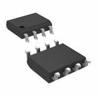
DS90LV001TM/NOPB National Semiconductor, DS90LV001TM/NOPB Datasheet

DS90LV001TM/NOPB
Specifications of DS90LV001TM/NOPB
*DS90LV001TM/NOPB
DS90LV001TM
Available stocks
Related parts for DS90LV001TM/NOPB
DS90LV001TM/NOPB Summary of contents
Page 1
... This will allow the device to also fill the role of an LVPECL-LVDS translator. Connection Diagram Block Diagram © 2008 National Semiconductor Corporation An output enable pin is provided, which allows the user to place the LVDS output in TRI-STATE. The DS90LV001 is offered in two package options pin LLP and SOIC ...
Page 2
... Absolute Maximum Ratings If Military/Aerospace specified devices are required, please contact the National Semiconductor Sales Office/ Distributors for availability and specifications. Supply Voltage ( LVCMOS/LVTTL Input Voltage (EN) LVDS Receiver Input Voltage (IN +, IN−) LVDS Driver Output Voltage (OUT +, OUT−) LVDS Output Short Circuit Current ...
Page 3
AC Electrical Characteristics Over recommended operating supply and temperature ranges unless otherwise specified. (Note 3) Symbol Parameter t Differential Propagation Delay High to Low PHLD t Differential Propagation Delay Low to High PLHD t Pulse Skew |t − ...
Page 4
DC Test Circuits FIGURE 2. Differential Driver Full Load DC Test Circuit AC Test Circuits and Timing Diagrams FIGURE 4. Propagation Delay Low-to-High and High-to-Low www.national.com FIGURE 1. Differential Driver DC Test Circuit FIGURE 3. LVDS Output Load 4 10133803 ...
Page 5
FIGURE 5. LVDS Output Transition Time FIGURE 6. TRI-STATE Delay Test Circuit FIGURE 7. Output active to TRI-STATE and TRI-STATE to active output time 10133809 10133804 5 10133801 www.national.com ...
Page 6
DS90LV001 Pin Descriptions (SOIC and LLP) Pin Name Pin # Input/Output GND 1 IN − OUT+ 6 OUT - DAP NA Typical Applications Backplane Stub-Hider Application www.national.com P Ground ...
Page 7
Cable Repeater Application Application Information MODE OF OPERATION The DS90LV001 can be used as a "stub-hider." In many sys- tems, signals are distributed across backplanes, and one of the limiting factors for system speed is the "stub length" or the ...
Page 8
Typical Performance Curves Output High Voltage vs Power Supply Voltage Output Short Circuit Current vs Power Supply Voltage www.national.com Output Low Voltage vs Power Supply Voltage 10133816 Differential Output Short Circuit Current vs Power Supply Voltage 10133818 8 10133817 10133819 ...
Page 9
Output TRI-STATE Current vs Power Supply Voltage 10133820 Differential Output Voltage vs Power Supply Voltage 10133822 Power Supply Current vs Frequency 10133824 Offset Voltage vs Power Supply Voltage Differential Output Voltage vs Load Resistor Power Supply Current vs Power Supply ...
Page 10
TRI-STATE Power Supply Current vs Power Supply Voltage Differential Propagation Delay vs Power Supply Voltage www.national.com Differential Transition Voltage vs Power Supply Voltage 10133826 Differential Propagation Delay vs Ambient Temperature 10133828 10 10133827 10133836 ...
Page 11
Differential Skew vs Power Supply Voltage 10133829 Transition Time vs Power Supply Voltage 10133830 Differential Skew vs Ambient Temperature Transition Time vs Ambient Temperature 11 10133837 10133838 www.national.com ...
Page 12
Differential Propagation Delay vs Differential Input Voltage Peak-to-Peak Output Jitter at V Differential Input Voltage www.national.com Differential Propagation Delay vs 10133831 = 0.4V vs Peak-to-Peak Output Jitter 10133833 12 Common-Mode Voltage 10133832 = 2. Differential ...
Page 13
Peak-to-Peak Output Jitter 1. Differential Input Voltage Peak-to-Peak Output Jitter at V Ambient Temperature 10133834 10133839 www.national.com ...
Page 14
Physical Dimensions www.national.com inches (millimeters) unless otherwise noted Order Number DS90LV001TM See NS Package Number M08A Order Number DS90LV001TLD See NS Package Number LDA08A 14 ...
Page 15
Notes 15 www.national.com ...
Page 16
... For more National Semiconductor product information and proven design tools, visit the following Web sites at: Products Amplifiers www.national.com/amplifiers Audio www.national.com/audio Clock Conditioners www.national.com/timing Data Converters www.national.com/adc Displays www.national.com/displays Ethernet www.national.com/ethernet Interface www.national.com/interface LVDS www.national.com/lvds Power Management www.national.com/power Switching Regulators www.national.com/switchers LDOs www ...


