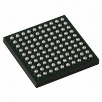
PI2EQX5804CNJE Pericom Semiconductor, PI2EQX5804CNJE Datasheet

PI2EQX5804CNJE
Specifications of PI2EQX5804CNJE
Available stocks
Related parts for PI2EQX5804CNJE
PI2EQX5804CNJE Summary of contents
Page 1
... PCIe® 2.0 ReDriver™ Description Pericom Semiconductor’s PI2EQX5804C is a low power, PCIe® compliant signal ReDriver™. The device provides programmable equalization, amplifi cation, and de-emphasis by using 8 select bits, to optimize performance over a variety of physical mediums by reducing Inter-symbol interference ...
Page 2
Pin # Pin Name Data Signals C4 A0RX+, B4 A0RX- C7 A0TX+, B7 A0TX- B1 A1RX+, C1 A1RX- B10 A1TX+, C10 A1TX- G3 A2RX+, G2 A2RX- G8 A2TX+, G9 A2TX- K2 A3RX+, K3 A3RX- K9 A3TX+, K8 A3TX- A8 B0RX+, ...
Page 3
Pin # Pin Name H5 DE_B F8 LB# G5 MODE C6 PD RESET# E10 RX50_A F1 RX50_B E7 RXD_A F4 RXD_B E6, E8 S[0:1]_A F5, F3 S[0:1]_B A5 SCL A6 SDA E1, E2, E3 SEL[0:2]_A ...
Page 4
Pin # Pin Name F10, F9, F7 SEL[0:2]_B E9 SIG_A F2 SIG_B Power Pins B2, B3, B8, B9, C2, C3, C8, C9, H2, GND H3, H8, H9, J2, J3, J8, J9 A1, A4, A7, A10, B6, D1, D4, D7, D10, ...
Page 5
Equalizer Confi guration The PI2EQX5804C input equalizer compensates for signal attenuation and Inter-Symbol Interference (ISI) re- sulting from long signal traces or cables, vias, signal crosstalk and other factors, by boosting the gain of high- frequency signal components. Because either ...
Page 6
Output Swing Control S1_[A:B] S0_[A: Emphasis settings are determined by the state of the DEx_y input pins and confi guration registers, as shown in the Output De-emphasis table below. De-Emphasis is selected ...
Page 7
The RESET# input is used to reset the receiver detect state machine to its initial state. The start of the receiver detect cycle starts when RESET# transitions from low to high. When a Receiver Detect cycle is begins the differential ...
Page 8
Loopback Operation Each lane of the PI2EQX5804C provides a loopback mode for test purposes which is controlled by a strapping 2 pin and I C register bit. The LB# pin controls all lanes together. When this pin is high normal ...
Page 9
I C Operation 2 The integrated I C interface operates as a slave device, supporting standard rate operation of 100Kbps, with 7-bit addressing mode. The data byte format is 8 bit bytes. The bytes must be accessed in sequential ...
Page 10
THE MOS-FET’S. The requirements for the most important characteristics of the MOS-FET’s, used as bi-directional level shifter. Type : N-channel enhancement mode MOS-FET. Gate threshold voltage : VGS(th) min. 0.8V max. 1.5V On resistance : RDS(on) max. 30 Ohm @ ...
Page 11
Transferring Data Every byte put on the SDA line must be 8-bits long. Each byte has to be followed by an acknowledge bit. Data is transferred with the most signifi cant bit (MSB) fi rst (see the I PI2EQX5804C will ...
Page 12
Register Description Byte 0 - Signal Detect (SIG) SIG_xy=0=low input signal, SIG_xy=1=valid input signal Bit 7 6 Name SIG_A0 SIG_B0 Type R R Power- State Note: R=Read only, W=Write only, R/W=Read and Write, X=Undefi ned, rsvd=reserved for future ...
Page 13
BYTE 3 - Channel Input Disable (INDIS) INDIS_xy=0=enable input, INDIS_xy=1=disable input Bit 7 6 Name INDIS_A0 INDIS_B0 Type R/W R/W Power- State Note: R=Read only, W=Write only, R/W=Read and Write, X=Undefi ned, rsvd=reserved for future use The Channel ...
Page 14
BYTE 6 - Power Down Control (PWR) PD_xy# =0=channel off/power down, PD_xy# =1=normal operation, Latch from PD# input at startup Bit 7 6 Name PD_A0# PD_B0# Type R/W R/W Power-on PD# PD# State Note: R=Read only, W=Write only, R/W=Read and ...
Page 15
Output Emphasis Confi guration earlier in this document for setting information. All four A channels get the same confi guration settings. BYTE 9 - B-Channels Equalizer and Output Control (BEOC) SELx_B: Equalizer confi guration, Dx_B: Emphasis control, Sx_B: Output ...
Page 16
I C Data Transfer 1. Read sequence ACK PI2EQX5804C Master DEV SEL 2. Write sequence ACK PI2EQX5804C Master DEV SEL 3. Combined sequence ACK PI2EQX5804C 2 I ...
Page 17
Maximum Ratings (Above which useful life may be impaired. For user guidelines, not tested.) Storage Temperature ...................................... Supply Voltage to Ground Potential........ –0.5V to +2.5V DC SIG Voltage....................................... –0. Current Output ........................................ –25mA to +25mA Power Dissipation Continuous ...
Page 18
Equalizer Symbol Parameter J Residual jitter RS-T J Residual jitter RS-D J Random jitter RM Notes 1. K28.7 pattern is applied differentially at point A as shown in AC test circuit (see fi gure). 2. Total jitter does not include ...
Page 19
SDA and SCL I/O for I C-bus Symbol Parameter V DC input logic high input logic low output logic low OL V Hysteresis of Schmitt trigger input hys Characteristics of the SDA and ...
Page 20
START SDA t SU;DAT LOW SCL t HD;STA t HD;DAT S 09-0001 5.0Gbps 4-Lane PCIe® 2.0 ReDriver™ with HD;STA t SU;STA HIGH Timing Channel Latency, 5.0 Gbps 20 PI2EQX5804C Equalization ...
Page 21
Output Level Settings (1V left, and 0.5V right at 5.0 Gbps) 0.0 dB (Dx = 000) –6.5 dB (Dx = 101) Output De-emphasis Characteristics 09-0001 5.0Gbps 4-Lane PCIe® 2.0 ReDriver™ with Equalization & Emphasis –3.5 dB (Dx = 010) –8.5 ...
Page 22
Eye Diagrams 5.0Gbps (input left, output right) Data Waveforms, 2.5Gbps (left) & 5.0Gbps (right) Signal Source Connector AC Test Circuit Referenced in the Electrical Characteristic Table 09-0001 5.0Gbps 4-Lane PCIe® 2.0 ReDriver™ with FR4 A B SmA SmA Connector ≤30 ...
Page 23
... Packaging Mechanical: 100-Ball LBGA (NJ) 08-0178 Ordering Information Ordering Number PI2EQX5804CNJE Notes: • Thermal characteristics can be found on the company web site at www.pericom.com/packaging/ • Pb-free and Green • X suffi Tape/Reel Pericom Semiconductor Corporation • 1-800-435-2336 • www.pericom.com 09-0001 ReDriver is a trademark of Pericom Semiconductor. ...


