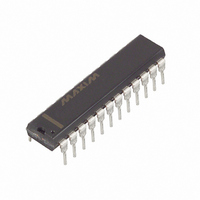
DS2176 Maxim Integrated Products, DS2176 Datasheet

DS2176
Specifications of DS2176
Available stocks
Related parts for DS2176
DS2176 Summary of contents
Page 1
... DS2176N DESCRIPTION The DS2176 is a low–power CMOS device specifically designed for synchronizing receive side loop– timed T–carrier data streams with system side timing. The device has several flexible operating modes which simplify interfacing incoming data to parallel and serial TDM backplanes. The device extracts, buffers and integrates ABCD signaling ...
Page 2
... DS2176 BLOCK DIAGRAM Figure DS2176 ...
Page 3
... System Serial Out. Updated on rising edge of SYSCLK. System Clock. 1.544 or 2.048 MHz data clock. System Clock Select. Tie to V 2.048 MHz. Positive Supply. 5.0 volts for parallel backplane applications select 193S(D4) framing low. SIGH for 1.544 MHz applications DS2176 for DD for DD ...
Page 4
... DATA SYNCHRONIZATION PCM BUFFER The DS2176 utilizes a 2–frame buffer (386 bits) to synchronize incoming PCM data to the system backplane clock. The buffer samples data at RSER on the falling edge of RCLK. Output data appears at SSER and is up-dated on the rising edge of SYSCLK. A rising edge at RMSYNC establishes receive side frame and multi-frame alignment. A rising edge at SFSYNC establishes system side frame alignment. The buffer depth is constantly monitored by onboard contention logic ...
Page 5
... MHz applications to compensate for the faster system-side read frequency. PARALLEL COMPATIBILITY The DS2176 is compatible with parallel and serial back-planes. Channel 1 data appears at SSER after a rising edge at SFSYNC as shown in Figures 3 and 4 (serial applications, S/ look–ahead circuit in parallel applications (S/ convert parallel data eternally ...
Page 6
... SYSTEM MULTIFRAME BOUNDARY TIMING (SYSCLK = 2.048 MHz) Figure 4 193S SYSTEM MULTIFRAME TIMING Figure 5 193E SYSTEM MULTIFRAME TIMING Figure DS2176 ...
Page 7
... PCM buffer (1 frame approximately 1 frame). INTEGRATION Signaling integration is another feature of the DS2176; when selected, it minimizes the impact of random noise hits on the span and resultant robbed–bit signaling corruption. Integration requires that per–channel signaling data be in the same state for two or more multiframes before appearing and D. SM0 and SM1 are used to select the degree of integration or to totally by-pass the feature ...
Page 8
... SSER with ones. 193E framing, no integration, 1 multiframe freeze, replace robbed bit signaling bits at SSER with ones. low may or may not cause a slip condition. ALN DS2176 ...
Page 9
... DS2176/DS2180A SYSTEM APPLICATION Figure 8 shows how the DS2180A T1 Transceiver and DS2176 Receive Buffer interconnect in a typical application. SERIAL 1.544 MHz BACKPLANE INTERFACE Figure DS2176 ...
Page 10
... C to +125 C 260 C for 10 seconds MIN TYP 4.5 DD MIN TYP - -1.0 LO MIN TYP out MAX UNITS NOTES V +0 +0.8 V 5.5 V (0°C to 70°C; V =5V ± 10%) DD MAX UNITS NOTES 10 mA +1.0 µ +1.0 µ MAX UNITS NOTES DS2176 1 ...
Page 11
... Output load capacitance = 100 pF. MIN TYP t RCLK 250 648 RWH, 125 324 t RWL t SWH, 100 244 t SWL 200 488 PVD t PSS PSF t SR 500 =5V DD MAX UNITS NOTES RWH SWH 100 100 DS2176 10%) ...
Page 12
... RECEIVE AC DIAGRAM Figure 9 SYSTEM AC TIMING DIAGRAM Figure DS2176 ...
Page 13
... DS2176 T1 RECEIVE BUFFER PKG 24-PIN DIM MIN MAX A IN. 1.245 1.265 MM B IN. 0.250 0.270 MM C IN. 0.125 0.145 MM D IN. 0.300 0.325 MM E IN. 0.015 0.040 MM F IN. 0.125 0.135 MM G IN. 0.090 0.110 MM H IN. 0.325 0.420 MM J IN. 0.008 0.012 MM K IN. 0.015 0.022 MM DS2176 ...
Page 14
... DS2176Q INCHES DIM MIN A 0.165 A1 0.090 A2 0.020 B 0.026 B1 0.013 C 0.009 D 0.485 D1 0.450 D2 0.390 E 0.485 E1 0.450 E2 0.390 L1 0.060 0.050 BSC CH1 0.042 MAX 0.180 0.120 - 0.033 0.021 0.012 0.495 0.456 0.430 0.495 0.456 0.430 - - 0.048 DS2176 ...
Page 15
... DATA SHEET REVISION SUMMARY The following represent the key differences between 04/19/95 and 06/13/97 version of the DS2176 data sheet. Please review this summary carefully. 1. SYNC/CLOCK Relationship in timing diagram DS2176 ...


