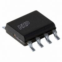
PCA9540BD,118 NXP Semiconductors, PCA9540BD,118 Datasheet - Page 5

PCA9540BD,118
Manufacturer Part Number
PCA9540BD,118
Description
IC I2C MUX 2CH 8-SOIC
Manufacturer
NXP Semiconductors
Datasheet
1.PCA9540BDP118.pdf
(22 pages)
Specifications of PCA9540BD,118
Package / Case
8-SOIC (3.9mm Width)
Applications
2-Channel I²C Multiplexer
Interface
I²C
Voltage - Supply
2.3 V ~ 3.6 V, 4.5 V ~ 5.5 V
Mounting Type
Surface Mount
Product
Decoders, Encoders, Multiplexers & Demultiplexers
Number Of Lines (input / Output)
2.0 / 1.0
Propagation Delay Time
0.3 ns at 2.3 V to 5.5 V
Supply Voltage (max)
5.5 V
Supply Voltage (min)
2.3 V
Maximum Operating Temperature
+ 85 C
Minimum Operating Temperature
- 40 C
Mounting Style
SMD/SMT
Number Of Input Lines
2.0
Number Of Output Lines
1.0
Lead Free Status / RoHS Status
Lead free / RoHS Compliant
For Use With
568-3615 - DEMO BOARD I2C
Lead Free Status / Rohs Status
Lead free / RoHS Compliant
Other names
568-1844-2
935276035118
PCA9540BD-T
935276035118
PCA9540BD-T
NXP Semiconductors
PCA9540B_4
Product data sheet
6.3 Power-on reset
6.4 Voltage translation
Table 3.
When power is applied to V
a reset condition until V
and the PCA9540B registers and I
states (all zeroes), causing all the channels to be deselected. Thereafter, V
lowered below 0.2 V to reset the device.
The pass gate transistors of the PCA9540B are constructed such that the V
be used to limit the maximum voltage that will be passed from one I
Figure 7
was generated using the data specified in
data sheet). In order for the PCA9540B to act as a voltage translator, the V
should be equal to, or lower than the lowest bus voltage. For example, if the main bus was
running at 5 V, and the downstream buses were 3.3 V and 2.7 V, then V
equal to or below 2.7 V to effectively clamp the downstream bus voltages. Looking at
D7
X
X
X
X
0
Fig 7.
(1) maximum
(2) typical
(3) minimum
D6
X
X
X
X
0
shows the voltage characteristics of the pass gate transistors (note that the graph
Pass gate voltage versus supply voltage
Control register: Write—channel selection; Read—channel status
D5
X
X
X
X
0
V
Rev. 04 — 3 September 2009
o(sw)
(V)
D4
X
X
X
X
0
DD
5.0
4.0
3.0
2.0
1.0
2.0
has reached V
DD
, an internal Power-On Reset (POR) holds the PCA9540B in
2.5
D3
X
X
X
X
0
2
C-bus state machine are initialized to their default
3.0
B2
0
1
1
1
0
POR
3.5
Section 10 “Static characteristics”
. At this point, the reset condition is released
B1
X
0
0
1
0
4.0
(1)
(2)
(3)
4.5
B0
X
0
1
X
0
002aaa964
5.0
V
2-channel I
DD
(V)
Command
no channel selected
channel 0 enabled
channel 1 enabled
no channel selected
no channel selected;
power-up default state
5.5
PCA9540B
2
C-bus to another.
2
C-bus multiplexer
© NXP B.V. 2009. All rights reserved.
o(sw)
DD
o(sw)
DD
should be
of this
voltage can
must be
voltage
5 of 22


