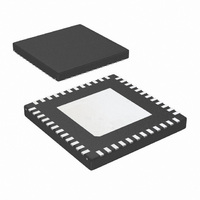
DS32EV400SQ/NOPB National Semiconductor, DS32EV400SQ/NOPB Datasheet - Page 6

DS32EV400SQ/NOPB
Manufacturer Part Number
DS32EV400SQ/NOPB
Description
IC EQUALIZER QUAD 3.2GBPS 48LLP
Manufacturer
National Semiconductor
Series
PowerWise®r
Datasheet
1.DS32EV400SQNOPB.pdf
(18 pages)
Specifications of DS32EV400SQ/NOPB
Applications
Signal Processing
Interface
Serial
Voltage - Supply
2.5V, 3.3V
Package / Case
48-LLP
Mounting Type
Surface Mount
For Use With
DS32EV400-EVK - KIT EVALUATION
Lead Free Status / RoHS Status
Lead free / RoHS Compliant
Other names
DS32EV400SQTR
www.national.com
SIGNAL DETECT and ENABLE TIMING
t
t
t
t
ZISD
IZSD
OZOED
ZOED
Note 1: “Absolute Maximum Ratings” indicate limits beyond which damage to the device may occur, including inoperability and degradation of device reliability
and/or performance. Functional operation of the device and/or non-degradation at the Absolute Maximum Ratings or other conditions beyond those indicated in
the Recommended Operating Conditions is not implied. The Recommended Operating Conditions indicate conditions at which the device is functional and the
device should not be operated beyond such conditions. Absolute Maximum Numbers are guaranteed for a junction temperature range of –40°C to +125°C. Models
are validated to Maximum Operating Voltages only.
Note 2: Typical values represent most likely parametric norms at V
characterization and are not guaranteed.
Note 3: The Electrical Characteristics tables list guaranteed specifications under the listed Recommended Operating Conditions except as otherwise modified
or specified by the Electrical Characteristics Conditions and/or Notes. Typical specifications are estimations only and are not guaranteed.
Note 4: Allowed supply noise (mV
Note 5: Specification is guaranteed by characterization and is not tested in production.
Note 6: Deterministic jitter is measured at the differential outputs (point C of Figure 1), minus the deterministic jitter before the test channel (point A of Figure 1).
Random jitter is removed through the use of averaging or similar means.
Note 7: Measured with clock like {11111 00000} pattern.
Note 8: Random jitter contributed by the equalizer is defined as sqrt (J
Figure 1; J
Note 9: The V
Symbol
IN
is the random jitter at the input of the equalizer in ps-rms, see Figure 1.
DD2.5
Input OFF to ON detect — SD
Output High Response Time
Input ON to OFF detect — SD
Output Low Response Time
EN High to Output ON Response
Time
EN Low to Output OFF Response
Time
is V
DD
= 2.5V ± 5% and V
Parameter
P-P
sine wave) under typical conditions.
DD3.3
is V
DD
= 3.3V ± 10%.
Response time measurement at
V
100 Mbps, 40” of 6 mil microstrip
FR4
Figure 1 Figure 4(Note
Response time measurement at
EN input to V
100 Mbps, 40” of 6 mil microstrip
FR4
Figure 1 Figure 5(Note
IN
to SD output, V
DD
= 3.3V, T
OUT
2
Conditions
− J
O
, V
IN
6
A
2
= 25°C, and at the Recommended Operation Conditions at the time of product
). J
IN
IN
OUT
= 800 mV
= 800 mV
is the random jitter at the equalizer outputs in ps-rms, see point C of
7)
7)
P-P
P-P
,
,
Min
((Note
Typ
400
150
35
5
2))
Max
Units
ns
ns
ns
ns


