LM93CIMT/NOPB National Semiconductor, LM93CIMT/NOPB Datasheet
LM93CIMT/NOPB
Specifications of LM93CIMT/NOPB
*LM93CIMT/NOPB
LM93CIMT
Available stocks


Related parts for LM93CIMT/NOPB

LM93CIMT/NOPB Summary of contents
Page 1
... Order Number NS Package Number Transport media LM93CIMT MTD56 LM93CIMTX MTD56 registered trademark of the Philips Corporation. © 2004 National Semiconductor Corporation n Dual dynamic VID monitoring (6 VIDs per processor general purpose I/Os: — 4 can be configured as fan tachometer inputs — 2 can be configured to connect to THERMTRIP from a processor — ...
Page 2
Block Diagram www.national.com 2 20068201 ...
Page 3
Application Baseboard management of a Dual processor server. Two LM93s may be required to manage a quad processor base- board. The block diagram of LM93 hardware is illustrated below. The hardware implementation is a single chip ASIC solution. 2 ...
Page 4
General Description ..................................................................................................................................... 1 2.0 Features ....................................................................................................................................................... 1 3.0 Key Specifications ........................................................................................................................................ 1 4.0 Applications .................................................................................................................................................. 1 5.0 Ordering Information .................................................................................................................................... 1 6.0 Block Diagram .............................................................................................................................................. 2 7.0 Application .................................................................................................................................................... 3 8.0 Connection Diagram .................................................................................................................................... 7 9.0 Pin Descriptions ...
Page 5
ERROR STATUS REGISTERS ............................................................................................................. 27 15.6.1 ASF Mode ........................................................................................................................................ 27 15.7 MASKING, ERROR STATUS AND ALERT ........................................................................................... 27 15.8 LAYOUT AND GROUNDING ................................................................................................................ 27 15.9 THERMAL DIODE APPLICATION ......................................................................................................... 27 15.9.1 Accuracy Effects of Diode Non-Ideality Factor ................................................................................ 28 ...
Page 6
Registers 90–AFh Voltage Limit Registers ................................................................................... 58 16.7.4 Register B0–B1h PROCHOT User Limit Registers ...................................................................... 59 16.7.5 Register B2–B3h Dynamic Vccp Limit Offset Registers ............................................................... 60 16.7.6 Register B4–BBh Fan Tach Limit Registers ................................................................................. 61 16.8 SETUP REGISTERS ............................................................................................................................. ...
Page 7
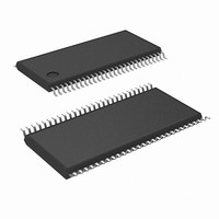
Connection Diagram 56 Pin TSSOP NS Package MTD56 Top View NS Order Numbers: LM93CIMT (34 units per rail), or LM93CIMTX (1000 units per tape-and-reel) 7 20068202 www.national.com ...
Page 8
Pin Descriptions Symbol Pin # Type GPIO_0/TACH1 1 Digital I/O (Open-Drain) GPIO_1/TACH2 2 Digital I/O (Open-Drain) GPIO_2/TACH3 3 Digital I/O (Open-Drain) GPIO_3/TACH4 4 Digital I/O (Open-Drain) GPIO_4 / 5 Digital I/O P1_THERMTRIP (Open-Drain) GPIO_5 / 6 Digital I/O P2_THERMTRIP ...
Page 9
Pin Descriptions (Continued) Symbol Pin # Type REMOTE2− 21 Remote Thermal Diode_2 - Input (CPU2 THERMDC) REMOTE2+ 22 Remote Thermal Diode_2 + I/O (CPU2 THERMDA) AD_IN1 23 Analog Input (+12V1) AD_IN2 24 Analog Input (+12V2) AD_IN3 25 Analog Input ...
Page 10
Pin Descriptions Symbol Pin # Type AD_IN16 39 POWER (V standby power GND 40 GROUND PWM1 41 Digital Output (Open-Drain) PWM2 42 Digital Output (Open-Drain) P1_VID0 43 Digital Input P1_VID1 44 Digital Input P1_VID2 45 Digital Input P1_VID3 46 ...
Page 11
Server Terminology MTTR Mean time to repair NIC Network Interface Card (Ethernet Card) OS Operating system P/S Power Supply PCI PCI Local Bus PDB Power Distribution Board 11.0 Recommended Implementation Note: 100 pF cap is optional and should be ...
Page 12
Functional Description The LM93 provides 16 channels of voltage monitoring, two remote thermal diode monitors, an onboard ambient tem- perature sensor, 2 PROCHOT monitors, 4 fan tachometers, 8 GPIOs, THERMTRIP monitor for masking error events, 2 SCSI_TERM inputs, and ...
Page 13
Functional Description (Continued) provide a nominal ⁄ full scale reading, while the −12V 3 4 should be scaled to provide a nominal thevenin resistance at the pin should be kept between 1 kΩ and 7 kΩ. The −12V monitoring ...
Page 14
Functional Description (Continued) Required External Level Shifting Resistors for −12V Power Input The +3.3V standby voltage is used as a reference for the level shifting. Therefore, the tolerance of this voltage directly effects the accuracy of the −12V reading. ...
Page 15
Functional Description (Continued) Value Register -11.6758 78 -11.6511 79 -11.6264 80 -11.6018 81 -11.5771 82 -11.5524 83 -11.5277 84 -11.5030 85 -11.4783 86 -11.4536 87 -11.4289 88 -11.4042 89 -11.3795 90 -11.3548 91 -11.3301 92 -11.3054 ...
Page 16
Functional Description (Continued) mented to a max count for an above temperature trip and decremented to zero when below the trip temperature set- ting, to remove the trip. The minimum time for PROCHOT assertion is time depen- dant on ...
Page 17
Functional Description (Continued) is configured to short the PROCHOT signals together, it always asserts them together whenever this function is en- abled. 12.12 FAN SPEED MEASUREMENT The fan tach circuitry measures the period of the fan pulses by enabling ...
Page 18
Inputs/Outputs (Continued) of these issues caused problems that were difficult to work around so moving to monitoring the fuse was selected as the solution. These inputs do not have to be used for monitoring SCSI fuses. Assertion of the ...
Page 19
SMBus Interface (Continued) telling the slave device to expect a block write may simply be a register address that tells the slave where sub- sequent data written. Since data can flow in only one ...
Page 20
SMBus Interface 14.5.2 Block Command Code Summary Block command codes control the block read and write operations of the LM93 as summarized in the following table: Command Code Name Block Write Command Block Read Command Fixed Block 0 Fixed ...
Page 21
SMBus Interface (Continued) 14.5.3.3 SMBus Write Block to Any Address The start address for a block write is embedded in this transaction. In this operation the master sends a block of data to the slave as follows: 1. The ...
Page 22
SMBus Interface 14.5.4 Read Operations The LM93 uses the following SMBus read protocols. 14.5.4.1 Read Byte In the LM93, the read byte protocol is used to read a single byte of data from a register. In this operation the ...
Page 23
SMBus Interface (Continued) 12. The master receives byte 1 and then asserts ACK. 13. The master receives byte 2 and then asserts ACK. 14. The master receives N-3 data bytes, and asserts ACK for each one. 15. The master ...
Page 24
SMBus Interface 14.5.4.4 Simulated SMBus Block-Write Block-Read Process Call Alternatively, if the master cannot support an SMBus Block-Write Block-Read process call, it can be emulated by two transactions (a block write followed by a block read). This should only ...
Page 25
SMBus Interface (Continued) 5. The master sends a repeated START. 6. The master sends the 7-bit slave address followed by a read bit (high). 7. The slave asserts an ACK. 8. The master receives the Byte Count (depends on ...
Page 26
SMBus Interface Whenever the low byte of a 16-bit register is written, the write is buffered and does not take effect until the corresponding high byte is written. If the low byte of a different 16-bit register is written, ...
Page 27
Using The LM93 (Continued) Channel Input Typical Assignment # 1 Temp Zone 1 Remote Diode 1 Temp Reading 2 Temp Zone 2 Remote Diode 2 Temp Reading 3 Temp Zone 3 Internal Temperature Reading 4 AIN1 +12V1 5 AIN2 ...
Page 28
Using The LM93 Thermal Diode Temperature vs. LM93 Temperature Reading 15.9.1 Accuracy Effects of Diode Non-Ideality Factor The technique used in today’s remote temperature sensors is to measure the change two different operating BE points of ...
Page 29
Using The LM93 (Continued) size and cost of the inductor and other components used in the output stage. The PWM outputs of the LM93 can operate up to 22.5 kHz with a step size of 6.25%. The LM93 fan ...
Page 30
Using The LM93 In this example: Zones 1 and 2 are bound to the PWM1 output and the PWM1 frequency set to a value in the low range; Hysteresis is set to 2˚C; Toffset and hysteresis resolution is set ...
Page 31
Using The LM93 (Continued) Note that since zones 1 and 2 share the same lookup table, both zones must be operating in the same resolution mode. The same applies to zones 3 and 4 since they share the same ...
Page 32
Using The LM93 15.10.8 VRDx_HOT Ramp-Up/Ramp-Down This function causes the duty cycle of the PWM outputs to gradually increase over time if VRD1_HOT or VRD2_HOT are asserted. When VRDx_HOT is asserted, the ramp function is enabled. The enabling process ...
Page 33
Using The LM93 (Continued) 15.11 XOR TREE TEST An XOR tree is provided in the LM93 for Automated Test Equipment (ATE) board level connectivity testing. This al- lows the functionality of all digital inputs to be tested in a ...
Page 34
Registers 16.1 REGISTER WARNINGS In most cases, reserved registers and register bits return zero when read. This should not be relied upon, since reserved registers can be used for future expansion of the LM93 functions. Some registers have “N/D” ...
Page 35
Registers (Continued) Lock Register Name VALUE REGISTERS Zone 2 (CPU2) Filtered Temp AD_IN1 Voltage AD_IN2 Voltage AD_IN3 Voltage AD_IN4 Voltage AD_IN5 Voltage AD_IN6 Voltage AD_IN7 Voltage AD_IN8 Voltage AD_IN9 Voltage AD_IN10 Voltage AD_IN11 Voltage AD_IN12 Voltage AD_IN13 Voltage AD_IN14 ...
Page 36
Registers (Continued) Lock Register Name LIMIT REGISTERS Zone 2 (CPU2) High Temp Zone 3 (Internal) Low Temp Zone 3 (Internal) High Temp Zone 4 (External Digital) Low Temp Zone 4 (External Digital) High Temp x Fan Boost Temp Zone ...
Page 37
Registers (Continued) Lock Register Name LIMIT REGISTERS P2_PROCHOT User Limit Vccp1 Limit Offsets Vccp2 Limit Offsets FAN Tach 1 Limit LSB FAN Tach 1 Limit MSB FAN Tach 2 Limit LSB FAN Tach 2 Limit MSB FAN Tach 3 ...
Page 38
Registers (Continued) Lock Register Name SETUP REGISTERS x Zone 1 Base Temperature x Zone 2 Base Temperature x Zone 3 Base Temperature x Zone 4 Base Temperature x Step 2 Temp Offset x Step 3 Temp Offset x Step ...
Page 39
Registers (Continued) Lock Register Name BLOCK COMMANDS Block Write Command Block Read Command Fixed Block 0 Fixed Block 1 Fixed Block 2 Fixed Block 3 Fixed Block 4 Fixed Block 5 Fixed Block 6 Fixed Block 7 Fixed Block ...
Page 40
Registers (Continued) 16.3 FACTORY REGISTERS 00h–3Fh 16.3.1 Register 00h XOR Test Register Read/ Register Address Write Name 00h R/W XOR Test Bit Name R/W Default 0 XEN R/W 0 The LM93 incorporates an XOR tree test mode. When the ...
Page 41
Registers (Continued) 16.4 BMC ERROR STATUS REGISTERS 40h–47h The B_Error Status Registers contain several bits that each represent a particular error event that the LM93 can monitor. The LM93 sets a given bit whenever the corresponding error event occurs. ...
Page 42
Registers (Continued) 16.4.2 Register 41h B_Error Status 2 Register Read/ Register Address Write Name B_Error ADIN8 41h RWC Status 2 _ERR Bit Name R/W 0 AD1_ERR RWC This bit is set when the AD_IN1 voltage has fallen outside the ...
Page 43
Registers (Continued) 16.4.4 Register 43h B_Error Status 4 Register Read/ Register Bit 7 Address Write Name B_Error D2_ 43h RWC Status 4 ERR Bit Name R/W 1:0 RES R Reserved 2 SCSI1_ERR RWC SCSI Fuse Error This bit is ...
Page 44
Registers (Continued) 16.4.6 Register 45h B_P2_PROCHOT Error Status Register Read/ Register Address Write Name B_P2_PROCHOT 45h RWC Error Status Bit Name R RWC Set when P2_PROCHOT has had a throttled event. This bit is set for any ...
Page 45
Registers (Continued) 16.4.8 Register 47h B_Fan Error Status Register Read/ Register Address Write Name B_Fan 47h RWC Error Status Bit Name R/W 0 FAN1_ERR RWC This bit is set when the Fan Tach 1 value register is above the ...
Page 46
Registers (Continued) 16.5.2 Register 49h H_Error Status 2 Register Read/ Register Address Write Name H_Error ADIN8 49h RWC Status 2 _ERR Bit Name R/W 0 AD1_ERR RWC This bit is set when the AD_IN1 voltage has fallen outside the ...
Page 47
Registers (Continued) 16.5.3 Register 4Ah H_Error Status 3 Register Read/ Register Bit 7 Address Write Name H_Error ADIN16 4Ah RWC Status 3 _ERR Bit Name R/W 0 AD9_ERR RWC This bit is set when the AD_IN9 voltage has fallen ...
Page 48
Registers (Continued) 16.5.4 Register 4Bh H_Error Status 4 Register Read/ Register Address Write Name H_Error 4Bh RWC Status 4 Bit Name R/W 1:0 RES R Reserved 2 SCSI1_ERR RWC SCSI Fuse Error This bit is set if SCSI_TERM1 has ...
Page 49
Registers (Continued) 16.5.5 Register 4Ch H_P1_PROCHOT Error Status Register Read/ Register Address Write Name H_P1_PROCHOT 4Ch RWC Error Status Bit Name R RWC Set when P1_PROCHOT has had a throttled event. This bit is set for any ...
Page 50
Registers (Continued) 16.5.6 Register 4Dh B_P2_PROCHOT Error Status Register Read/ Register Address Write Name H_P2_PROCHOT 4Dh RWC Error Status Bit Name R RWC Set when P2_PROCHOT has had a throttled event. This bit is set for any ...
Page 51
Registers (Continued) 16.5.7 Register 4Eh H_GPI Error Status Register Read/ Register Address Write Name H_GPI 4Eh RWC Error Status Bit Name R/W 0 GPI0_ERR RWC This bit is set whenever GPIO0 is driven low (unless masked via the GPI ...
Page 52
Registers (Continued) 16.5.8 Register 4Fh H_Fan Error Status Register Read/ Register Address Write Name H_Fan 4Fh RWC Error Status Bit Name R/W 0 FAN1_ERR RWC This bit is set when the Fan Tach 1 value register is above the ...
Page 53
Registers (Continued) 16.6.3 Register 56–65h A/D Channel Voltage Registers Register Read/ Register Address Write Name 56h R AD_IN1 Voltage 57h R AD_IN2 Voltage 58h R AD_IN3 Voltage 59h R AD_IN4 Voltage 5Ah R AD_IN5 Voltage 5Bh R AD_IN6 Voltage ...
Page 54
Registers (Continued) 16.6.5 Register 68h Average P1_PROCHOT Register Read/ Register Address Write Name Average 68h R P1_PROCHOT This is the average percentage active time of P1_PROCHOT the result of adding the contents of this register to the ...
Page 55
Registers (Continued) 16.6.8 Register 6Bh GPI State Register Read/ Register Address Write Name 6Bh R GPI State Bit Name 0 GPI0 1 GPI1 2 GPI2 3 GPI3 4 GPI4 5 GPI5 6 GPI6 7 GPI7 16.6.9 Register 6Ch P1_VID ...
Page 56
Registers (Continued) 16.6.11 Register 6E–75h Fan Tachometer Readings Register Read/ Register Bit 7 Address Write Name Fan Tach 6Eh R 1 LSB Fan Tach 6Fh R 1 MSB Fan Tach 70h R 2 LSB Fan Tach 71h R 2 ...
Page 57
Registers (Continued) 16.7 LIMIT REGISTERS 16.7.1 Registers 78–7Fh Temperature Limit Registers Register Read/ Register Address Write Name Processor 1 (Zone1) 78h R/W Low Temp Processor 1 (Zone1) 79h R/W High Temp Processor 2 (Zone2) 7Ah R/W Low Temp Processor ...
Page 58
Registers (Continued) 16.7.3 Registers 90–AFh Voltage Limit Registers Register Read/ Register Address Write Name 90h R/W AD_IN1 Low Limit 91h R/W AD_IN1 High Limit 92h R/W AD_IN2 Low Limit 93h R/W AD_IN2 High Limit 94h R/W AD_IN3 Low Limit ...
Page 59
Registers (Continued) 16.7.4 Register B0–B1h PROCHOT User Limit Registers Register Read/ Register Address Write Name P1_PROCHOT B0h R/W User Limit P2_PROCHOT B1h R/W User Limit These registers allow a user limit to be set for the PROCHOT monitoring function. ...
Page 60
Registers (Continued) 16.7.5 Register B2–B3h Dynamic Vccp Limit Offset Registers Register Read/ Register Address Write Name B2h R/W Vccp1 Limit Offsets B3h R/W Vccp2 Limit Offsets These offsets are used to determine the upper and lower limits of the ...
Page 61
Registers (Continued) 16.7.6 Register B4–BBh Fan Tach Limit Registers Register Read/ Register Address Write Name Fan Tach 1 B4h R/W Limit LSB Fan Tach 1 B5h R/W Limit MSB Fan Tach 2 B6h R/W Limit LSB Fan Tach 2 ...
Page 62
Registers (Continued) 16.8 SETUP REGISTERS 16.8.1 Register BCh Special Function Control 1 (Voltage Hysteresis and Fan Control Filter Enable) Register Read/ Register Address Write Name Special Function BCh R/W Control 1 Bit Name R/W 2:0 VH R/W Voltage hysteresis ...
Page 63
Registers (Continued) 16.8.2 Register BDh Special Function Control 2 (Smart Tach Mode Enable and Fan Control Temperature Resolution Control) Register Read/ Register Address Write Name Special Function BDh R/W Control 2 Bit Name 0 STE1 1 STE2 2 STE3 ...
Page 64
Registers (Continued) 16.8.4 Register BFh PWM Ramp Control Register Read/ Register Address Write Name PWM Ramp BFh R/W Control Bit Name 3:0 VRD_RAMP 7:4 PH_RAMP If the time delay between steps is set to 0 ms, the PWM duty ...
Page 65
Registers (Continued) 16.8.6 Register C1h Fan Boost Hysteresis (Zones 3/4) Register Read/ Register Address Write Name Fan Boost C1h R/W Hysteresis (Zones 3/4) Bit Name 3 the temperature zone is above fan boost temperature and ...
Page 66
Registers (Continued) 16.8.8 Register C3h Zones 1/2 MinPWM and Hysteresis Register Read/ Register Address Write Name Zones 1/2 C3h R/W MinPWM and Hysteresis Bit Name 3:0 FC_TH 7:4 MinPWM 16.8.9 Register C4h Zones 3/4 MinPWM and Hysteresis Register Read/ ...
Page 67
Registers (Continued) 16.8.10 Register C5h GPO Register Read/ Register Bit 7 Address Write Name C5h R/W GPO GPO7 Bit Name 0 GPO0 1 GPO1 2 GPO2 3 GPO3 4 GPO4 5 GPO5 6 GPO6 7 GPO7 Bit 6 Bit ...
Page 68
Registers (Continued) 16.8.11 Register C6h PROCHOT Override Register Read/ Register Address Write Name PROCHOT C6h R/W Override Bit Name 3:0 PHT_DC 5:4 RES 6 FORCE_P1 7 FORCE_P2 Note that if the P1P2_PROCHOT bit is set to short the Px_PROCHOT ...
Page 69
Registers (Continued) 16.8.12 Register C7h PROCHOT Time Interval Register Read/ Register Address Write Name PROCHOT C7h R/W Time Interval Bit Name 3:0 P1_TI 7:4 P2_TI Possible settings for P1_TI and P2_TI: P1_TI or P2_TI Note that changing this value ...
Page 70
Registers (Continued) 16.8.13 Register C8h PWM1 Control 1 Register Read/ Register Address Write Name PWM1 C8h R/W Control 1 Bit Name 0 ZN1 1 ZN2 2 ZNE 3 ZN4 4 PH1 5 PH2 6 VRD1 7 VRD2 This register ...
Page 71
Registers (Continued) 16.8.14 Register C9h PWM1 Control 2 Register Read/ Register Address Write Name PWM1 C9h R/W Control 2 Bit Name 0 OVR 1 INV 2 EPPL 3 PPL 7:4 OVR_DC Bit 7 Bit 6 Bit 5 Bit 4 ...
Page 72
Registers (Continued) 16.8.15 Register CAh PWM1 Control 3 Register Read/ Register Address Write Name PWM1 CAh R/W Control 3 Bit Name 3:0 SU_DC 4 RES 7:5 SU_DUR Bits 7:5 configure the spin-up duration. When the duty cycle of PWM1 ...
Page 73
Registers (Continued) 16.8.17 Register CCh PWM2 Control 1 Register Read/ Register Address Write Name PWM2 CCh R/W Control 1 Bit Name 0 ZN1 1 ZN2 2 ZN3 3 ZN4 4 PH1 5 PH2 6 VRD1 7 VRD2 This register ...
Page 74
Registers (Continued) 16.8.18 Register CDh PWM2 Control 2 Register Read/ Register Address Write Name PWM2 CDh R/W Control 2 Bit Name 0 OVR 1 INV 2 EPPL 3 PPL 7:4 OVR_DC www.national.com Bit 7 Bit 6 Bit 5 Bit ...
Page 75
Registers (Continued) 16.8.19 Register CEh PWM2 Control 3 Register Read/ Register Address Write Name PWM2 CEh R/W Control 3 Bit Name 3:0 SU_DC 4 RES 7:5 SU_DUR Bits 7:5 configure the spin-up duration. When the duty cycle of PWM2 ...
Page 76
Registers (Continued) 16.8.21 Register D0h–D3h Zone Base Temperatures Register Read/ Register Address Write Name Zone 1 Base D0h R/W Temperature Zone 2 Base D1h R/W Temperature Zone 3 Base D2h R/W Temperature Zone 4 Base D3h ...
Page 77
Registers (Continued) 16.8.23 Register E0h Special Function TACH to PWM Binding Register Read/ Register Address Write Name Special Function E0h R/W TACH to PWM Binding Bit Name 0 T1P1 1 T1P2 2 T2P1 3 T2P2 4 T3P1 5 T3P2 ...
Page 78
Registers (Continued) 16.8.24 Register E2h LM93 Status Control Register Read/ Register Bit 7 Address Write Name LM93 Status/ BMC E2h R/W Control _ERR Lock Bit Name 0 OVRID X 1 ASF 2 GPI4_AM 3 GP15_AM 5:4 TACH_EDGE 6 HOST_ERR ...
Page 79
Registers (Continued) 16.8.25 Register E3h LM93 Configuration Register Read/ Register Address Write Name LM93 E3h R/W READY Configuration Lock Bit Name x 0 START X 1 LOCK 2 GMSK 3 ALERT_EN 4 P1P2_ PROCHOT 6:5 RES 7 READY Bit ...
Page 80
Registers (Continued) 16.9 SLEEP STATE CONTROL AND MASK REGISTERS 16.9.1 Register E4h Sleep State Control Register Read/ Register Address Write Name Sleep State E4h R Control Bit Name 1:0 SB 7:2 RES www.national.com Bit 7 Bit 6 Bit 5 ...
Page 81
Registers (Continued) 16.9.2 Register E5h S1 GPI Mask Register Read/ Register Bit 7 Address Write Name S1 GPI GPI7_S1 E5h R/W Mask _MSK Bit Name 0 GPI0_S1_MSK 1 GPI1_S1_MSK 2 GPI2_S1_MSK 3 GPI3_S1_MSK 4 GPI4_S1_MSK 5 GPI5_S1_MSK 6 GPI6_S1_MSK ...
Page 82
Registers (Continued) 16.9.4 Register E7h S3 GPI Mask Register Read/ Register Bit 7 Address Write Name S3 GPI GPI7_S3 E7h R/W Mask _MSK Bit Name 0 GPI0_S3_MSK 1 GPI1_S3_MSK 2 GPI2_S3_MSK 3 GPI3_S3_MSK 4 GPI4_S3_MSK 5 GPI5_S3_MSK 6 GPI6_S3_MSK ...
Page 83
Registers (Continued) 16.9.7 Register EAh S4/5 GPI Mask Register Read/ Register Address Write Name GPI7 S4/5 GPI EAh R/W _S4/5 Mask _MSK Bit Name 0 GPI0_S4/5_MSK 1 GPI1_S4/5_MSK 2 GPI2_S4/5_MSK 3 GPI3_S4/5_MSK 4 GPI4_S4/5_MSK 5 GPI5_S4/5_MSK 6 GPI6_S4/5_MSK 7 ...
Page 84
Registers (Continued) 16.10 OTHER MASK REGISTERS 16.10.1 Register ECh GPI Error Mask Register Read/ Register Address Write Name GPI Error ECh R/W Mask Bit Name 0 GPI0_MSK 1 GPI1_MSK 2 GPI2_MSK 3 GPI3_MSK 4 GPI4_MSK 5 GPI5_MSK 6 GPI6_MSK ...
Page 85
Registers (Continued) 16.10.3 Register EEh Special Function Zone 1 Adjustment Offset Register Read/ Register Address Write Name Special Function EEh R/W Zone 1 Adjustment Offset Bit Name 5:0 Z1_ADJUST 7:6 RES 16.10.4 Register EFh Special Function Zone 2 Adjustment ...
Page 86
... Absolute Maximum Ratings (Notes Military/Aerospace specified devices are required, please contact the National Semiconductor Sales Office/ Distributors for availability and specifications. Positive Supply Voltage ( Voltage on Any Digital Input or Output Pin Voltage on +5V Input Voltage at Positive Thermal ± Diode Inputs, 12V Inputs − ...
Page 87
DC Electrical Characteristics The following limits apply for +3 the operating range; all other limits T MAX LM93 the junction temperature of the LM93 Symbol Parameter DNL Differential Non-Linearity PSS Power Supply ...
Page 88
AC Electrical Characteristics The following limits apply for +3 the operating range; all other limits T MAX Symbol Parameter FAN RPM-TO-DIGITAL CHARACTERISTICS Counter Resolution Number of fan tach pulses count is based on Counter Frequency Accuracy PWM ...
Page 89
Note 1: Absolute Maximum Ratings indicate limits beyond which damage to the device may occur. Operating Ratings indicate conditions for which the device is functional, but do not guarantee specific performance limits. For guaranteed specifications and test conditions, see the ...
Page 90
Symbol Pin # AD_IN1 23 AD_IN2 24 AD_IN3 25 AD_IN4 26 AD_IN5 27 AD_IN6 28 AD_IN7 29 AD_IN8 30 AD_IN9 31 AD_IN10 32 AD_IN11 33 AD_IN12 34 AD_IN13 35 AD_IN14 36 AD_IN15 37 ADDR_SEL 38 AD_IN16 (V+) GND ...
Page 91
Note 15: Timing specifications are tested at the TTL logic levels 1.4V. 19.0 Data Sheet Version History Version Date 2.0 April 12, 2004 1. Updated Section 16.7.2 Registers 80–83h Fan Boost Temperature Registers, changed "If set to 80h, ...
Page 92
... BANNED SUBSTANCE COMPLIANCE National Semiconductor certifies that the products and packing materials meet the provisions of the Customer Products Stewardship Specification (CSP-9-111C2) and the Banned Substances and Materials of Interest Specification (CSP-9-111S2) and contain no ‘‘Banned Substances’’ as defined in CSP-9-111S2. ...