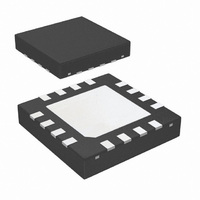
LMH0384SQE/NOPB National Semiconductor, LMH0384SQE/NOPB Datasheet - Page 3

LMH0384SQE/NOPB
Manufacturer Part Number
LMH0384SQE/NOPB
Description
IC ADAPT CBL EQUALIZER 16-LLP
Manufacturer
National Semiconductor
Datasheet
1.LMH0384SQENOPB.pdf
(16 pages)
Specifications of LMH0384SQE/NOPB
Applications
Digital Interface
Interface
SPI
Voltage - Supply
3.135 V ~ 3.465 V
Package / Case
16-LLP
Mounting Type
Surface Mount
Leaded Process Compatible
Yes
Rohs Compliant
Yes
Input Voltage
3.3 V
Supply Voltage (max)
3.45 V
Supply Voltage (min)
3.15 V
Maximum Operating Temperature
+ 85 C
Minimum Operating Temperature
- 40 C
Mounting Style
SMD/SMT
Peak Reflow Compatible (260 C)
Yes
Lead Free Status / RoHS Status
Lead free / RoHS Compliant
Other names
LMH0384SQETR
Available stocks
Company
Part Number
Manufacturer
Quantity
Price
Company:
Part Number:
LMH0384SQE/NOPB
Manufacturer:
STM
Quantity:
4 302
Symbol Parameter
BR
BR
t
t
RL
R
C
Symbol Parameter
Recommended Input Timing Requirements
f
t
t
t
t
t
t
t
Switching Characteristics
t
t
t
r
OS
SCK
PH
PL
SU
H
SSSU
SSH
SSOF
ODZ
OZD
OD
,t
IN
IN
AC Electrical Characteristics
Over Supply Voltage and Operating Temperature ranges, unless otherwise specified (Note 3).
SPI Interface AC Electrical Characteristics
Over Supply Voltage and Operating Temperature ranges, unless otherwise specified (Note 3).
Note 1: "Absolute Maximum Ratings" are those parameter values beyond which the life and operation of the device cannot be guaranteed. The stating herein of
these maximums shall not be construed to imply that the device can or should be operated at or beyond these values. The table of "Electrical Characteristics"
specifies acceptable device operating conditions.
Note 2: Current flow into device pins is defined as positive. Current flow out of device pins is defined as negative. All voltages are stated referenced to
V
Note 3: Typical values are stated for V
Note 4: Specification is guaranteed by characterization.
Note 5: The LMH0384 can be optimized for different launch amplitudes via the SPI.
f
IN
MIN
MAX
EE
= 0 Volts.
Minimum Input Data Rate
Maximum Input Data Rate
Jitter for Various Cable Lengths
Output Rise Time, Fall Time
Mismatch in Rise/Fall Time
Output Overshoot
Input Return Loss
Input Resistance
Input Capacitance
SCK Frequency
SCK Pulse Width High
SCK Pulse Width Low
MOSI Setup Time
MOSI Hold Time
SS Setup Time
SS Hold Time
SS Off Time
MISO Driven-to-Tristate Time
MISO Tristate-to-Driven Time
MISO Output Delay Time
CC
= +3.3V and T
Conditions
270 Mbps, Belden 1694A,
0-350 meters (Note 8)
270 Mbps, Belden 1694A,
350-400 meters
1.485 Gbps, Belden 1694A,
0-170 meters (Note 8)
1.485 Gbps, Belden 1694A,
170-200 meters
2.97 Gbps, Belden 1694A,
0-110 meters (Note 8)
2.97 Gbps, Belden 1694A,
110-140 meters
20% – 80%, 100Ω load, (Note
4), Figure 1
(Note 4)
(Note 4)
5 MHz - 1.5 GHz, (Note 9)
1.5 GHz - 3.0 GHz, (Note 9)
single-ended
single-ended
Conditions
Figures 2, 3
Figures 2, 3
Figures 2, 3
Figure 3
A
= +25°C.
3
Reference
SDI, SDI
SDO, SDO
SDI, SDI
Reference
SCK
MOSI
SS
MISO
Min
Min
15
10
40
40
10
4
4
4
4
0.35
Typ
125
Typ
0.2
0.3
1.3
0.7
80
2
1
2970
Max
0.25
Max
130
0.2
0.3
15
20
15
15
15
5
www.national.com
% SCK
% SCK
period
period
Units
Mbps
Mbps
Units
MHz
dB
dB
kΩ
ps
ps
pF
ns
ns
ns
ns
ns
ns
ns
ns
UI
UI
UI
UI
UI
UI
%


