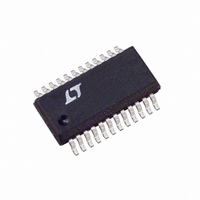
LTC1755EGN Linear Technology, LTC1755EGN Datasheet

LTC1755EGN
Specifications of LTC1755EGN
Available stocks
Related parts for LTC1755EGN
LTC1755EGN Summary of contents
Page 1
... Battery life is maximized operating current and 1 A shutdown current. The narrow SSOP packages mini- mize PCB area for compact portable systems. , LTC and LT are registered trademarks of Linear Technology Corporation. 3.3V 1 PRES 2 PWR ...
Page 2
... U (Note 1) CLK, RST, I/O, AUX1, AUX2 to GND .............................. – 0. Short-Circuit Duration ............................... Indefinite CC Operating Temperature Range (Note 2) .. – Storage Temperature Range ................ – 150 C + 0.3V Lead Temperature (Soldering, 10 sec)................. 300 0. ORDER PART NUMBER TOP VIEW LTC1755EGN PRES 1 PWR 2 GND I/O 6 RST 7 8 CLK GN PACKAGE ...
Page 3
ELECTRICAL CHARACTERISTICS temperature range, otherwise specificatons are at T PARAMETER LTC1755 (V = 2. 5.5V, unless otherwise noted Operating Voltage IN DV Operating Voltage CC I Operating Current VIN I Operating ...
Page 4
LTC1755/LTC1756 ELECTRICAL CHARACTERISTICS temperature range, otherwise specificatons are at T PARAMETER Controller Inputs/Outputs DATA, AUX1IN, AUX2IN, DV High Input Voltage Threshold ( Low Input Voltage Threshold ( High Level Output Voltage ( Low Level ...
Page 5
W U TYPICAL PERFOR A CE CHARACTERISTICS Power Efficiency vs Input Voltage 100 I = 35mA INPUT ...
Page 6
LTC1755/LTC1756 W U TYPICAL PERFOR A CE CHARACTERISTICS Supply Current Shutdown 9 7.5 6.0 4.5 3.0 1 INPUT VOLTAGE (V) ...
Page 7
CTIO S LTC1755/LTC1756 Note normally closed switch is used, a small current (several microamperes) will flow through the switch when- ever a Smart Card is not present. For ultralow power consumption in shutdown, ...
Page 8
LTC1755/LTC1756 CTIO S LTC1755/LTC1756 microseconds then the LTC1755/LTC1756 switch to the Alarm state. This fault checking is only performed after the V pin has reached its final value (as indicated by the CC READY pin). ...
Page 9
CTIO S LTC1755/LTC1756 The READY pin is configured as an open-drain pull-down with a weak pull-up current source. This permits wired- OR connections of multiple LTC1755/LTC1756s to a single microcontroller. ALARM (Pin 22, LTC1755 Only): ...
Page 10
LTC1755/LTC1756 W BLOCK DIAGRA DV CC PRES PWR CS (LTC1755 ONLY) NC/NO (LTC1755 ONLY) GND AUX1 (LTC1755 ONLY) * AUX2 (LTC1755 ONLY) * I/O RST CLK * DYNAMIC PULL-UP CURRENT SOURCE 10 DC/DC CONVERTER AND ...
Page 11
U U APPLICATIO S I FOR ATIO 10kV ESD Protection All Smart Card pins (CLK, RST, I/O, AUX1, AUX2, V GND) can withstand over 10kV of human body model ESD in situ. In order to ensure proper ESD protection, careful ...
Page 12
LTC1755/LTC1756 U U APPLICATIO S I FOR ATIO released by comparing its slew rate with an internal reference value valid transition is detected, a large pull-up current enhances the edge rate on the node. The higher slew rate ...
Page 13
U U APPLICATIO S I FOR ATIO Compatibility 2 Some smart cards still require I C compatibility. In the I format it is permissible to impose an L before the signal line has returned H. This ...
Page 14
LTC1755/LTC1756 U U APPLICATIO S I FOR ATIO Overtemperature Fault Protection An overtemperature circuit disables the chip and activates the ALARM pin if the IC’s junction temperature exceeds 150 C. Self-Start Mode By connecting the CARD pin to the PWR ...
Page 15
... FLASH SHALL NOT EXCEED 0.010" (0.254mm) PER SIDE Information furnished by Linear Technology Corporation is believed to be accurate and reliable. However, no responsibility is assumed for its use. Linear Technology Corporation makes no represen- tation that the interconnection of its circuits as described herein will not infringe on existing patent rights. ...
Page 16
... Output from Input, S0-8 Package Step-Up/Step-Down Charge Pump + Generates from 2.7V to 5.5V, 50mA Output with from 2.6V to 4.4V, 3V/5V Output at 10mA – C CONTROLLER C1 0. DATA 10 RIN 9 CIN 17556 TA02 from 2V to 10V, SO-8 Package sn17556a 17556fs LT/LCG 0800 4K • PRINTED IN USA LINEAR TECHNOLOGY CORPORATION 1999 ...


