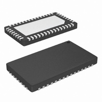
QLX4300SIQSR Intersil, QLX4300SIQSR Datasheet

QLX4300SIQSR
Specifications of QLX4300SIQSR
Related parts for QLX4300SIQSR
QLX4300SIQSR Summary of contents
Page 1
... CAUTION: These devices are sensitive to electrostatic discharge; follow proper IC Handling Procedures. | 1-888-INTERSIL or 1-888-468-3774 Intersil (and design registered trademark of Intersil Americas Inc. All other trademarks mentioned are the property of their respective owners. Copyright Intersil Americas Inc. 2009. All Rights Reserved ...
Page 2
... PART MARKING QLX4300SIQT7 QLX4300SIQ QLX4300SIQSR QLX4300SIQ NOTE: These Intersil Pb-free plastic packaged products employ special Pb-free material sets; molding compounds/die attach materials and NiPdAu plate - e4 termination finish, which is RoHS compliant and compatible with both SnPb and Pb-free soldering operations. Intersil Pb-free products are MSL classified at Pb-free peak reflow temperatures that meet or exceed the Pb-free requirements of IPC/JEDEC J STD-020 ...
Page 3
Pin Descrptions PIN NAME PIN NUMBER DT 1 Detection Threshold. Reference DC current threshold for input signal power detection. Data output OUT[k] is muted when the power of the equalized version of IN[k] falls below the threshold. Tie to ground ...
Page 4
Pin Descrptions (Continued) PIN NAME PIN NUMBER OUT2[N,P] 33, 34 Equalizer 2 differential output, CML. The use of 100nF low ESL/ESR MLCC capacitor with at least 4GHz frequency response is recommended. OUT1[N,P] 36, 37 Equalizer 1 differential output, CML. The ...
Page 5
... Thermal Resistance (Typical QFN Package (Note 1 Operating Ambient Temperature Range 0°C to +70°C Storage Ambient Temperature Range . . . . . -55°C to +150°C Maximum Junction Temperature +125°C Pb-Free Reflow Profile see link below http://www.intersil.com/pbfree/Pb-FreeReflow.asp CONDITION NRZ data applied to any channel Typical values are ...
Page 6
Electrical Specifications Typical values are PARAMETERS SYMBOL Input Return Loss (Com. to Diff. Conversion) Output Amplitude Range V OUT Differential Output Impedance Output Return Loss (Differential) Output Return Loss S 22 ...
Page 7
NOTES: (Continued) 10. During line silence, transmitter noise in excess of this voltage range may result in differential output amplitudes from the QLx4300-S45 that are greater than 20mV 11. The data pattern preceding line silence mode is comprised of the ...
Page 8
Typical Performance Characteristics FIGURE 2. JITTER VS BOOST SETTING FOR VARIOUS CABLE LENGTHS, PRBS-7, 0.03PS SYSTEM JITTER INCLUDED OUTPUT EYE DIAGRAMS 64ps/div FIGURE 3. RECEIVED SIGNAL AFTER 10m OF 26AWG TWIN-AXIAL CABLE, 3.125Gb/s 64ps/div FIGURE 5. RECEIVED SIGNAL AFTER 15m ...
Page 9
Typical Performance Characteristics 64ps/div FIGURE 7. RECEIVED SIGNAL AFTER 20m OF 26AWG TWIN-AXIAL CABLE, 3.125Gb/s 64ps/div FIGURE 9. RECEIVED SIGNAL AFTER 25m OF 26AWG TWIN-AXIAL CABLE, 3.125Gb/s RETURN LOSS AND CROSSTALK CHARACTERISTICS 0 Channel 1 -5 Channel 2 Channel 3 ...
Page 10
Typical Performance Characteristics 0 -5 -10 -15 -20 -25 -30 -35 0 0.5 1 1.5 2 Frequency (GHz) FIGURE 13. INPUT DIFFERENTIAL RETURN LOSS FIGURE 15. DIFFERENTIAL CROSSTALK BETWEEN ADJACENT INPUT CHANNEL Operation The QLx4300-S45 is an advanced quad lane-extender ...
Page 11
CP[k] pins are used to set the level. The equalizer transfer functions for a subset of these compensation levels are plotted in Figure 18. The flexibility of this adjustable ...
Page 12
Channel Power-Down In addition to controlling the input impedance, the IS[k] pin powers down the equalizer channel when pulled low. This feature allows a system controller individually to power down unused channels and to minimize power consumption. Example: the signal ...
Page 13
Equalization Boost Level Channel equalization for the QLx4300-S45 can be individually set to either (a) one of 18 levels through the DC voltages on external control pins or (b) one of 32 levels via a set of registers programmed by ...
Page 14
Optimal Cable Boost Settings The settable equalizing filter within the QLx4300-S45 enables the device to optimally compensate for frequency-dependent attenuation across a wide variety of channels, data rates, and encoding schemes. For the reference channels plotted in Figure 2, Table ...
Page 15
ENB t CLK DI FIGURE 22. TIMING DIAGRAM FOR PROGRAMMING THE INTERNAL REGISTERS OF THE QLx4300-S45 Serial Bus Programming Pins 16 (DI), 45 (ENB), and 46 (CLK) are used to program the registers inside the QLx4300-S45. Figure 22 shows an ...
Page 16
Serial Register Data QLx4300-S45 (A) ENB DI CLK DO Clock ENB (A) FIGURE 23. SERIAL BUS PROGRAMMING MULTIPLE QLx4300-S45 DEVICES USING SEPARATE ENB SIGNALS ENB t SCK CLK DO FIGURE 24. TIMING DIAGRAM FOR DI/DO CARRYOVER Serial Register Data QLx4300-S45 ...
Page 17
ENB t SCK CLK t t SDI HDI DI R21 R20 QLx4300-S45 (D) FIGURE 26. TIMING DIAGRAM FOR PROGRAMMING MULTIPLE QLx4300-S45 DEVICES USING DI/DO CARRYOVER Detection Thereshold (DT) Pin Functionality The QLx4300-S45 is capable of maintaining periods of line silence ...
Page 18
Typical Application Reference Designs Figures 28 and 29 show reference design schematics for a QLx4300-S45 evaluation board with an SMA connector interface. Figure 28 shows the schematic for the case when the equalizer boost level is set via the CP ...
Page 19
Typical Application Reference Designs Figures 28 and 29 show reference design schematics for a QLx4300-S45 evaluation board with an SMA connector interface. Figure 28 shows the schematic for the case when the equalizer boost level is set via the CP ...
Page 20
... Accordingly, the reader is cautioned to verify that data sheets are current before placing orders. Information furnished by Intersil is believed to be accurate and reliable. However, no responsibility is assumed by Intersil or its subsidiaries for its use; nor for any infringements of patents or other rights of third parties which may result from its use. No license is granted by implication or otherwise under any patent or patent rights of Intersil or its subsidiaries ...
Page 21
Package Outline Drawing L46.4x7 46 LEAD THIN QUAD FLAT NO-LEAD PLASTIC PACKAGE (TQFN) Rev 0, 9/09 4.00 6 PIN 1 INDEX AREA (4X) 0.05 TOP VIEW 0.70 ±0.05 SIDE VIEW ( 3. 2.50 5.50 ...


